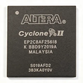
EPM570F256C3N - MAX II CPLD, 570 LEs, 256-FBGA | Intel / Altera
部品番号: EPM570F256C3N ✓ 生産中| 数量 | 単価 | 小計 |
|---|---|---|
| 1 | $19.98 | $19.98 |
| 10 | $18.5 | $185.00 |
| 100 | $16.8 | $1,680.00 |
| 500 | $15.2 | $7,600.00 |
| 1,000 | $13.75 | $13,750.00 |
EPM570F256C3N 概要
A MAX II CPLD is a Complex Programmable Logic Device: a non-volatile, instantly-on programmable logic IC that combines the deterministic timing and ease of use of a traditional PAL/GAL-style device with the density and feature integration of modern FPGAs. Unlike SRAM-based FPGAs, MAX II devices store their configuration in on-chip flash, eliminating the need for external boot PROMs and enabling instant-on behavior at power-up. Within the broader programmable-logic taxonomy, MAX II sits below low-cost FPGAs in density but above simple SPLDs in capability, occupying a unique space for glue-logic, I/O expansion, bus bridging, and power-sequencing tasks.
The EPM570F256C3N provides up to 212 user I/O pins (package-dependent), four MultiVolt I/O banks, and enhanced in-system programmability (ISP) compliant with IEEE 1532 / IEEE 1149.1 JTAG. Designers can choose between commercial and industrial temperature grades; the 'C3N' suffix indicates a commercial-grade device (0C to +85C), with the on-chip flash configuration setting it apart from SRAM-based competitors.
Typical applications for the EPM570F256C3N include system-level glue logic in industrial controllers, I/O expansion and voltage-level translation between mixed-voltage ASICs/ASICs, register-based bus interface bridging, power-supply sequencing and supervisory logic, and LED-driving and display-control functions. The on-chip UFM can also be used to store user parameters, calibration constants, or board ID data.
When designing with this device, ensure that JTAG chain integrity is preserved, observe MultiVolt bank VCCIO constraints when mixing voltage domains, and leverage the Quartus Prime design tools (free MAX II support) for synthesis, fitting, and programming-file generation.
This page synthesizes distributor pricing from LCSC and Xecor, drop-in alternative MPNs from the same MAX II family and across competitors, and practical design notes not found in the manufacturer datasheet alone.
ドロップイン代替品: EPM570F256C3N — 同一パッケージでピン互換。PCBの作り直しが必要な異なるパッケージの部品は除外されています。
このシリーズのバリエーション
同一シリーズでドロップイン互換のモデル: EPM570F256C3N (同一形状・フットプリント) — 相違点: Package, Programming Interface, Operating Temperature, Process Technology, RoHS Status.
クイック比較ツール — 並列比較する代替部品を選択:
EPM570F256C4N
✅ ドロップイン✓ 在庫あり
$26.85 / 個
データシートを見る →EPM570F256C3
✅ ドロップイン✓ 在庫あり
$14.85 / 個
データシートを見る →EPM570F256I5N
✅ ドロップイン✓ 在庫あり
$19.85 / 個
データシートを見る →EPM570F256C3N 最大定格&電気的特性
| Family | MAX II |
| Logic Elements (LEs) | 570 |
| Equivalent Macrocells | 440 |
| User Flash Memory (UFM) | 8 Kbits |
| Maximum Operating Frequency | 304 MHz |
| Process Technology | 0.18 um, 6-layer-metal flash CMOS |
| Core Voltage | 2.5 V / 3.3 V |
| I/O Voltage Support (MultiVolt) | 1.5 V, 1.8 V, 2.5 V, 3.3 V |
| パッケージ | 256-ball FBGA (FineLine BGA) |
| Operating Temperature (C3 grade) | 0 C to +85 C (commercial) |
| Programming Interface | JTAG (IEEE 1532 / IEEE 1149.1) + ISP |
| 実装タイプ | Surface Mount |
| RoHS ステータス | Compliant (per DigiKey listing) |
| Lead-Free | Yes (per suffix 'N' convention) |
| Typical Macroscopic Functions | Glue logic, bus bridging, I/O expansion, power sequencing |
EPM570F256C3N 256-ball fbga (fineline bga) ピン配置ガイド
EPM570F256C3N (256-ball fbga (fineline bga) パッケージ) のピン配置。 このデジタルICには、GPIO、通信インターフェース (UART、SPI、I2C)、および電源ピンが含まれています。代替ピン機能と設定オプションについては、メーカーのデータシートを参照してください。組み込みシステム設計とPCBレイアウトに不可欠です。

詳細なピン配置データはありません: EPM570F256C3N.
詳細は データシート をご参照ください。
主な用途
EPM570F256C3N の用途: 6 件s: Industrial Control - Glue Logic, I/O Expansion & Voltage-Level Translation, Power-Supply Sequencing & Supervisory Logic, Bus Interface Bridging, LED Driving & Display Control, Consumer Appliance Interface Boards.
Industrial Control - Glue Logic
The EPM570F256C3N excels as glue logic in industrial controllers where 570 LEs and 212 user I/Os are sufficient to replace 4-8 discrete PAL/GAL devices and slow ASICS. Its non-volatile flash configuration gives instant-on behavior at machine startup, eliminating the FPGA-style boot-PROM and external reset-sequencer overhead that industrial PLCs and motor-control boards usually carry. With 4 MultiVolt I/O banks, the device bridges between 5V-tolerant legacy sensors, 3.3V MCUs, and 1.8V FPGAs on the same PCB without external level shifters, reducing BOM and assembly cost. Designers use the on-chip 8 Kbit UFM to store factory calibration constants and machine IDs that survive power-cycle and field-update scenarios.
おすすめ
I/O Expansion & Voltage-Level Translation
The EPM570F256C3N's MultiVolt I/O architecture makes it ideal for voltage-level translation between mixed-voltage ASICs/MCUs in compact designs. Each of the four I/O banks supports 1.5V, 1.8V, 2.5V, or 3.3V independently, so a single CPLD can simultaneously interface a 1.8V application processor, 2.5V DDR memory, 3.3V peripheral bus, and 5V-tolerant industrial I/O. With 570 LEs designers can implement bidirectional buffers, uni-/bi-directional voltage translators, and protocol bridges (I2C to SPI, UART to parallel) in one device. The non-volatile configuration means translation logic is live within microseconds of power-up, critical for systems where downstream devices cannot tolerate long reset windows.
おすすめ
Power-Supply Sequencing & Supervisory Logic
The EPM570F256C3N is widely used as a multi-rail power sequencer in networking, server, and telecom boards where multiple voltage rails must come up in a specific order. With 570 LEs the device can implement more than 24 PG (power-good) comparator inputs, programmable delay chains, fault latching, and I2C/PMBus status reporting - replacing a stack of discrete supervisory ICs. The on-chip UFM stores rail-order configuration, fault logs, and board-revision codes that survive field updates. Quartus Prime's deterministic timing (pin-to-pin delays locked at compile time) is critical for sequencing accuracy, and the JTAG/ISP chain enables in-system firmware updates without removing the board from service.
おすすめ
Bus Interface Bridging
In legacy-modern interface bridging - for example, between an MCU's local bus and a parallel FPGA bus, or between an SPI flash and a 16-bit camera bus - the EPM570F256C3N delivers deterministic sub-3 ns pin-to-pin delays that simplify timing closure. Its 570 LEs are enough to implement small FIFOs, address decoders, and protocol state machines for bridges such as SPI-to-parallel, I2C-to-GPIO, or UART-to-LCD. The JTAG/ISP chain plus Quartus Prime support make design iteration fast, and the on-chip UFM can store protocol personality tables that swap bridge behavior without re-spinning the PCB.
おすすめ
LED Driving & Display Control
The EPM570F256C3N is well-suited to drive LED matrices, segment displays, and small character LCDs because its 212 user I/Os can sink/source substantial per-pin current and its MultiVolt banks can drive both 3.3V logic-level LEDs and 5V common-anode displays directly. With 570 LEs designers can implement charlieplex decoding, PWM dimming, and blanking-interval control in a single device, replacing microcontrollers whose timers cannot keep up with high-refresh-rate multiplexing. The flash-based configuration is ideal for commercial signage and consumer appliances where instant-on blink patterns must run before the host MCU is ready.
おすすめ
Consumer Appliance Interface Boards
Consumer appliance mainboards - washing machines, induction cooktops, air-conditioner indoor units - often need a flexible logic block to interface the user keypad, rotary encoder, LED indicators, and the main appliance MCU. The EPM570F256C3N with 570 LEs and 212 user I/Os handles 7-segment displays, encoder debouncing, and buzzer/timer patterns in one device, while its non-volatile flash configuration means the interface is fully functional within microseconds of power-on - even before the appliance MCU boots. The commercial-grade temperature profile and BGA-256 footprint make it a cost-effective, board-space-efficient choice for high-volume appliance production.
おすすめ
おすすめ製品の概要
エンジニアリング参考データ: EPM570F256C3N — 比較、設計ガイダンス、コンプライアンス情報。
選定ガイド
代替品との比較
| パラメータ | この製品 | EPM570F256C4N | EPM570F256C3 | EPM570F256I5N |
|---|---|---|---|---|
| Brand | Intel (formerly Altera) | Intel | Intel | Intel |
| Package | 256-FBGA (FineLine BGA) | 256-FBGA - same | 256-FBGA - same | 256-FBGA - same |
| Logic Elements (LEs) | 570 | 570 - same | 570 - same | 570 - same |
| Equivalent Macrocells | 440 | 440 - same | 440 - same | 440 - same |
| User Flash Memory (UFM) | 8 Kbits | 8 Kbits | 8 Kbits | 8 Kbits |
| Speed Grade / Pin-to-Pin Delay | C3 (commercial, ~3 ns class) | C4 (faster, 4 ns commercial) | C3 (same speed grade) | I5 (industrial, 5 ns) |
| Operating Temperature | 0 C to +85 C (commercial) | 0 C to +85 C (commercial) | 0 C to +85 C (commercial) | -40 C to +100 C (industrial) |
| Core Voltage | 2.5 V / 3.3 V | 2.5 V / 3.3 V | 2.5 V / 3.3 V | 2.5 V / 3.3 V |
主な差別化要因
- Non-volatile flash configuration with instant-on behavior (vs SRAM-based CPLD competitors (e.g., Xilinx XC-9500XL))
- MultiVolt I/O banks (1.5V / 1.8V / 2.5V / 3.3V) (vs Single-voltage I/O CPLDs (e.g., older MAX 7000))
- On-chip 8 Kbit User Flash Memory (UFM) (vs Most competing CPLDs lack integrated UFM)
設計ノート
The 256-ball FBGA package demands a 4- or 6-layer PCB with matched-length impedance control on high-speed I/O runs. Place the CPLD near the connectors or devices it bridges, route each MultiVolt I/O bank to a single voltage domain, and keep JTAG TMS/TCK/TDO/TDI traces short (< 50 mm) to avoid signal-integrity issues. Decoupling: place 0.1 uF X7R ceramics on every VCCINT and VCCIO pin, plus a single 10 uF bulk tantalum/ceramic per voltage rail within 25 mm of the package.
Each MultiVolt I/O bank can be powered independently; tie unused bank VCCIO pins to the lowest voltage in use on the board to minimize leakage. The MAX II VCCINT pin requires a clean 2.5V or 3.3V supply (per device variant); switching noise above 50 mVpp can couple into the JTAG scan chain and cause ISP failures. Estimated: at 304 MHz toggle rate with all 212 I/Os active, the EPM570F256C3N can draw up to ~150 mA from VCCINT; verify with the IBIS model during simulation.
Do not assume the C3N speed grade and the I5N speed grade are interchangeable: the I5N runs slower pin-to-pin but covers industrial temperature; mixing them in production can cause timing violations at temperature extremes. Always check the Quartus Prime fitter report's Slow 1200 mV / 85C and Fast 1200 mV / 0C corners. Also note that MAX II devices require the JTAG TCK line to be pulled up; a floating TCK can prevent ISP from initializing on some programmer cables.
コンプライアンス情報
RoHS and lead-free status inferred from 'N' suffix and DigiKey product listing. REACH, halogen-free, and conflict-minerals compliance not explicitly stated in the provided web data.