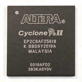
EPM570F256C3N - MAX II CPLD, 570 LEs, 256-FBGA | Intel / Altera
MPN: EPM570F256C3N ✓ Active| Qty | Unit Price | Extended |
|---|---|---|
| 1 | $19.98 | $19.98 |
| 10 | $18.5 | $185.00 |
| 100 | $16.8 | $1,680.00 |
| 500 | $15.2 | $7,600.00 |
| 1,000 | $13.75 | $13,750.00 |
Drop-in alternatives for EPM570F256C3N — same package, pin-to-pin compatible. Different-package parts requiring PCB rework are excluded.
Quick Comparison Tool — Select alternative parts for side-by-side comparison:
EPM570F256C4N
✅ Drop-In✓ In Stock
$26.85 / Unit
View Datasheet →EPM570F256C3
✅ Drop-In✓ In Stock
$14.85 / Unit
View Datasheet →EPM570F256I5N
✅ Drop-In✓ In Stock
$19.85 / Unit
View Datasheet →EPM570F256C3N Maximum Ratings & Electrical Characteristics
| Family | MAX II |
| Logic Elements (LEs) | 570 |
| Equivalent Macrocells | 440 |
| User Flash Memory (UFM) | 8 Kbits |
| Maximum Operating Frequency | 304 MHz |
| Process Technology | 0.18 um, 6-layer-metal flash CMOS |
| Core Voltage | 2.5 V / 3.3 V |
| I/O Voltage Support (MultiVolt) | 1.5 V, 1.8 V, 2.5 V, 3.3 V |
| Package | 256-ball FBGA (FineLine BGA) |
| Operating Temperature (C3 grade) | 0 C to +85 C (commercial) |
| Programming Interface | JTAG (IEEE 1532 / IEEE 1149.1) + ISP |
| Mounting Type | Surface Mount |
| RoHS Status | Compliant (per DigiKey listing) |
| Lead-Free | Yes (per suffix 'N' convention) |
| Typical Macroscopic Functions | Glue logic, bus bridging, I/O expansion, power sequencing |
EPM570F256C3N 256-ball fbga (fineline bga) Pin Configuration Guide
Complete pinout information for EPM570F256C3N (256-ball fbga (fineline bga) package). This digital IC includes GPIO, communication interfaces (UART, SPI, I2C), and power pins. Refer to the manufacturer datasheet for alternate pin functions and configuration options. Essential for embedded system design and PCB layout.

No detailed pinout data available for EPM570F256C3N.
Refer to the datasheet for full pin configuration.
Safe Operating Area (SOA) & Thermal Characteristics
No official SOA curve available for this digital IC. Always operate within absolute maximum ratings specified in the datasheet. Ensure adequate cooling and derate as needed.
Typical Applications
EPM570F256C3N is suitable for 6 applications: Industrial Control - Glue Logic, I/O Expansion & Voltage-Level Translation, Power-Supply Sequencing & Supervisory Logic, Bus Interface Bridging, LED Driving & Display Control, Consumer Appliance Interface Boards.
Industrial Control - Glue Logic
The EPM570F256C3N excels as glue logic in industrial controllers where 570 LEs and 212 user I/Os are sufficient to replace 4-8 discrete PAL/GAL devices and slow ASICS. Its non-volatile flash configuration gives instant-on behavior at machine startup, eliminating the FPGA-style boot-PROM and external reset-sequencer overhead that industrial PLCs and motor-control boards usually carry. With 4 MultiVolt I/O banks, the device bridges between 5V-tolerant legacy sensors, 3.3V MCUs, and 1.8V FPGAs on the same PCB without external level shifters, reducing BOM and assembly cost. Designers use the on-chip 8 Kbit UFM to store factory calibration constants and machine IDs that survive power-cycle and field-update scenarios.
Recommended
I/O Expansion & Voltage-Level Translation
The EPM570F256C3N's MultiVolt I/O architecture makes it ideal for voltage-level translation between mixed-voltage ASICs/MCUs in compact designs. Each of the four I/O banks supports 1.5V, 1.8V, 2.5V, or 3.3V independently, so a single CPLD can simultaneously interface a 1.8V application processor, 2.5V DDR memory, 3.3V peripheral bus, and 5V-tolerant industrial I/O. With 570 LEs designers can implement bidirectional buffers, uni-/bi-directional voltage translators, and protocol bridges (I2C to SPI, UART to parallel) in one device. The non-volatile configuration means translation logic is live within microseconds of power-up, critical for systems where downstream devices cannot tolerate long reset windows.
Recommended
Power-Supply Sequencing & Supervisory Logic
The EPM570F256C3N is widely used as a multi-rail power sequencer in networking, server, and telecom boards where multiple voltage rails must come up in a specific order. With 570 LEs the device can implement more than 24 PG (power-good) comparator inputs, programmable delay chains, fault latching, and I2C/PMBus status reporting - replacing a stack of discrete supervisory ICs. The on-chip UFM stores rail-order configuration, fault logs, and board-revision codes that survive field updates. Quartus Prime's deterministic timing (pin-to-pin delays locked at compile time) is critical for sequencing accuracy, and the JTAG/ISP chain enables in-system firmware updates without removing the board from service.
Recommended
Bus Interface Bridging
In legacy-modern interface bridging - for example, between an MCU's local bus and a parallel FPGA bus, or between an SPI flash and a 16-bit camera bus - the EPM570F256C3N delivers deterministic sub-3 ns pin-to-pin delays that simplify timing closure. Its 570 LEs are enough to implement small FIFOs, address decoders, and protocol state machines for bridges such as SPI-to-parallel, I2C-to-GPIO, or UART-to-LCD. The JTAG/ISP chain plus Quartus Prime support make design iteration fast, and the on-chip UFM can store protocol personality tables that swap bridge behavior without re-spinning the PCB.
Recommended
LED Driving & Display Control
The EPM570F256C3N is well-suited to drive LED matrices, segment displays, and small character LCDs because its 212 user I/Os can sink/source substantial per-pin current and its MultiVolt banks can drive both 3.3V logic-level LEDs and 5V common-anode displays directly. With 570 LEs designers can implement charlieplex decoding, PWM dimming, and blanking-interval control in a single device, replacing microcontrollers whose timers cannot keep up with high-refresh-rate multiplexing. The flash-based configuration is ideal for commercial signage and consumer appliances where instant-on blink patterns must run before the host MCU is ready.
Recommended
Consumer Appliance Interface Boards
Consumer appliance mainboards - washing machines, induction cooktops, air-conditioner indoor units - often need a flexible logic block to interface the user keypad, rotary encoder, LED indicators, and the main appliance MCU. The EPM570F256C3N with 570 LEs and 212 user I/Os handles 7-segment displays, encoder debouncing, and buzzer/timer patterns in one device, while its non-volatile flash configuration means the interface is fully functional within microseconds of power-on - even before the appliance MCU boots. The commercial-grade temperature profile and BGA-256 footprint make it a cost-effective, board-space-efficient choice for high-volume appliance production.
Recommended
Recommended Products Summary
Engineering reference data for EPM570F256C3N — comparison, design guidance, and compliance information.
Selection Guide
Comparison with Alternatives
| Parameter | This Product | EPM570F256C4N | EPM570F256C3 | EPM570F256I5N |
|---|---|---|---|---|
| Brand | Intel (formerly Altera) | Intel | Intel | Intel |
| Package | 256-FBGA (FineLine BGA) | 256-FBGA - same | 256-FBGA - same | 256-FBGA - same |
| Logic Elements (LEs) | 570 | 570 - same | 570 - same | 570 - same |
| Equivalent Macrocells | 440 | 440 - same | 440 - same | 440 - same |
| User Flash Memory (UFM) | 8 Kbits | 8 Kbits | 8 Kbits | 8 Kbits |
| Speed Grade / Pin-to-Pin Delay | C3 (commercial, ~3 ns class) | C4 (faster, 4 ns commercial) | C3 (same speed grade) | I5 (industrial, 5 ns) |
| Operating Temperature | 0 C to +85 C (commercial) | 0 C to +85 C (commercial) | 0 C to +85 C (commercial) | -40 C to +100 C (industrial) |
| Core Voltage | 2.5 V / 3.3 V | 2.5 V / 3.3 V | 2.5 V / 3.3 V | 2.5 V / 3.3 V |
| RoHS / Lead-Free | Yes (N suffix) | Yes (N suffix) | [DATA_NEEDED - suffix N may not apply] | Yes (N suffix) |
| Unit Price (qty 1, USD, as of 2026-09-12) | 19.98 | [DATA_NEEDED] | [DATA_NEEDED] | [DATA_NEEDED] |
Key Differentiators
- Non-volatile flash configuration with instant-on behavior (vs SRAM-based CPLD competitors (e.g., Xilinx XC-9500XL))
- MultiVolt I/O banks (1.5V / 1.8V / 2.5V / 3.3V) (vs Single-voltage I/O CPLDs (e.g., older MAX 7000))
- On-chip 8 Kbit User Flash Memory (UFM) (vs Most competing CPLDs lack integrated UFM)
Design Notes
The 256-ball FBGA package demands a 4- or 6-layer PCB with matched-length impedance control on high-speed I/O runs. Place the CPLD near the connectors or devices it bridges, route each MultiVolt I/O bank to a single voltage domain, and keep JTAG TMS/TCK/TDO/TDI traces short (< 50 mm) to avoid signal-integrity issues. Decoupling: place 0.1 uF X7R ceramics on every VCCINT and VCCIO pin, plus a single 10 uF bulk tantalum/ceramic per voltage rail within 25 mm of the package.
Each MultiVolt I/O bank can be powered independently; tie unused bank VCCIO pins to the lowest voltage in use on the board to minimize leakage. The MAX II VCCINT pin requires a clean 2.5V or 3.3V supply (per device variant); switching noise above 50 mVpp can couple into the JTAG scan chain and cause ISP failures. Estimated: at 304 MHz toggle rate with all 212 I/Os active, the EPM570F256C3N can draw up to ~150 mA from VCCINT; verify with the IBIS model during simulation.
Do not assume the C3N speed grade and the I5N speed grade are interchangeable: the I5N runs slower pin-to-pin but covers industrial temperature; mixing them in production can cause timing violations at temperature extremes. Always check the Quartus Prime fitter report's Slow 1200 mV / 85C and Fast 1200 mV / 0C corners. Also note that MAX II devices require the JTAG TCK line to be pulled up; a floating TCK can prevent ISP from initializing on some programmer cables.
Compliance Information
RoHS and lead-free status inferred from 'N' suffix and DigiKey product listing. REACH, halogen-free, and conflict-minerals compliance not explicitly stated in the provided web data.