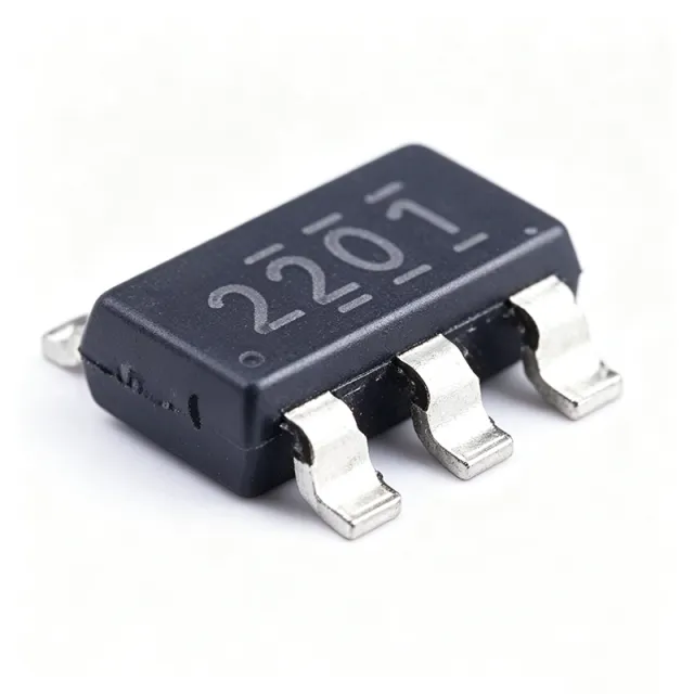
TPS562201DDCT - 2A 17V Sync Buck Converter | Texas Instruments
部品番号: TPS562201DDCT ✓ 生産中| 数量 | 単価 | 小計 |
|---|---|---|
| 1 | $0.68 | $0.68 |
| 10 | $0.61 | $6.10 |
| 100 | $0.55 | $55.00 |
| 500 | $0.49 | $245.00 |
| 1,000 | $0.45 | $450.00 |
TPS562201DDCT 概要
A DC-DC switching regulator converts a higher input voltage to a lower regulated output using power switches and an inductor, offering far higher efficiency than a linear regulator. Within the power management IC hierarchy, the TPS562201 belongs to the synchronous buck converter family and is part of TI's D-CAP2 controller portfolio for point-of-load (POL) rails.
Key features include the D-CAP2 control architecture, which provides fast transient response and supports both low-ESR and ceramic output capacitors with internal compensation, so no complex loop design is needed. Eco-mode pulse-skip operation maintains high efficiency at light loads by reducing switching frequency, while the 580 kHz fixed frequency allows small inductors and capacitors.
Technically, the internally compensated adaptive on-time loop reacts within microseconds to load steps, making the part well suited to processor core and I/O rails. Internal soft-start limits inrush current, and the device is specified over a -40C to +125C junction temperature range in the 2.9 mm x 1.6 mm SOT-23-Thin package.
Typical applications include 5V and 12V distributed-power point-of-load regulation, networking and telecom equipment, industrial automation systems, set-top boxes, and digital TV power supplies, where the 17V maximum input accepts 12V rails with headroom.
Design consideration: keep the output voltage within the 0.768V to 7V range and use the datasheet-recommended ceramic output capacitance for D-CAP2 stability; place input decoupling capacitors as close as possible to the VIN and GND pins.
This page synthesizes distributor pricing, drop-in alternatives, and practical design notes not found in the manufacturer datasheet.
ドロップイン代替品: TPS562201DDCT — 同一パッケージでピン互換。PCBの作り直しが必要な異なるパッケージの部品は除外されています。
このシリーズのバリエーション
同一シリーズでドロップイン互換のモデル: TPS562201DDCT (同一形状・フットプリント) — 相違点: Maximum Output Current, Output Voltage Range, Package, Input Voltage Range, Topology.
クイック比較ツール — 並列比較する代替部品を選択:
TPS562208DDCR
✅ ドロップイン📋 参考代替品(カタログ未掲載)
TPS562200DDCR
✅ ドロップイン📋 参考代替品(カタログ未掲載)
TPS563207DRLR
✅ ドロップイン ⚠️ 仕様未検証✓ 在庫あり
$0.31 / 個
データシートを見る →TPS563201DDCR
✅ ドロップイン ⚠️ 仕様未検証📋 参考代替品(カタログ未掲載)
TPS561201DDCR
✅ ドロップイン ⚠️ 仕様未検証✓ 在庫あり
$0.29 / 個
データシートを見る →TPS562201DDCT 最大定格&電気的特性
| トポロジー | Synchronous step-down (buck) |
| 入力電圧範囲 | 4.5 V to 17 V |
| 出力電圧範囲 | 0.768 V to 7 V (adjustable) |
| 最大出力電流 | 2 A |
| スイッチング周波数 | 580 kHz (fixed) |
| Control Scheme | D-CAP2 (adaptive on-time, internally compensated) |
| Light Load Mode | Eco-mode pulse-skip |
| Integrated MOSFETs | High-side and low-side FETs (synchronous) |
| 出力数 | 1 |
| 動作温度 | -40C to +125C (junction) |
| パッケージ | SOT-23-Thin (TSOT-23-6, DDC), 2.9 mm x 1.6 mm |
| 実装タイプ | Surface Mount |
| 帰還電圧 | 0.768 V |
| Protection Features | Internal soft-start, overcurrent protection |
| RoHS ステータス | Compliant |
| Packaging | Cut Tape (DDCT) / Tape & Reel (DDCR) |
TPS562201DDCT ピン構成
| ピン 1 | BOOT — Bootstrap capacitor connection for high-side gate driver |
| ピン 2 | GND — Ground reference |
| ピン 3 | SW — Switch node - connect to output inductor |
| ピン 4 | VIN — Input supply, 4.5 V to 17 V |
| ピン 5 | FB — Feedback input - resistor divider from VOUT |
| ピン 6 | EN — Enable pin (do not float; tie high or low) |
主な用途
TPS562201DDCT の用途: 6 件s: 12V Distributed Power Point-of-Load, Networking and Telecom Equipment, Industrial Automation Systems, Set-Top Boxes and Digital TV, SSD and Storage Peripheral Power, IoT and Smart Home Hubs.
12V Distributed Power Point-of-Load
The TPS562201DDCT is a natural fit for point-of-load regulation on 12V distributed power buses. Its 4.5V to 17V input range directly accepts 12V rails with margin for bus tolerance, and the 0.768V to 7V adjustable output covers 1.0V, 1.2V, 1.8V, 2.5V, 3.3V, and 5V logic rails. The D-CAP2 control loop provides fast transient response for dynamic processor loads, while the 580 kHz frequency keeps the inductor small. In a typical 12V-to-3.3V, 2A configuration, the synchronous topology maintains high efficiency without an external Schottky diode, and the 2.9 mm x 1.6 mm SOT-23-Thin package fits directly under dense BGA footprints.
おすすめ
Networking and Telecom Equipment
Switches, routers, and telecom line cards commonly run from 12V backplane feeds and need multiple efficient local rails. The TPS562201DDCT's 17V maximum input covers these buses directly, and Eco-mode pulse-skip operation keeps standby efficiency high when ports are idle - important for energy-efficient Ethernet and green-datacenter requirements. The D-CAP2 architecture handles the fast load steps that occur when port PHYs power up, and the internally compensated loop eliminates external compensation components, reducing BOM count on high-density line cards. Its 580 kHz fixed frequency also keeps switching noise out of sensitive baseband bands, and the -40C to +125C junction range suits unventilated telecom enclosures.
おすすめ
Industrial Automation Systems
Industrial controllers, sensors, and I/O modules require robust, wide-input, small-footprint power conversion. The TPS562201DDCT tolerates the supply variation typical of 24V-derived 12V auxiliary buses, and internal soft-start plus overcurrent protection simplify qualification for factory environments. The D-CAP2 loop's fast transient response supports FPGA and MCU loads that step between sleep and active modes, while Eco-mode keeps light-load draw low in always-on monitoring nodes. The 1.6 mm x 2.9 mm package and minimal external component count enable compact designs on standard industrial PCBs, and the -40C cold-start rating matches unheated cabinet installations common in factory automation deployments.
おすすめ
Set-Top Boxes and Digital TV
Set-top box and digital TV power architectures historically standardized on the D-CAP2 SOT-23 converter family, and the TPS562201DDCT is designed exactly for this market. It efficiently generates the 1.1V to 1.8V core rails for SoC decoders and the 3.3V/5V I/O rails from a single 12V adapter input. Eco-mode pulse-skip maintains regulatory light-load efficiency targets when the box is in standby, and the 580 kHz switching frequency keeps components small enough for the tight layouts inside consumer enclosures. The internally compensated loop handles the sharp current transitions when the decoder wakes, avoiding voltage droop that could reset the SoC during channel changes.
おすすめ
SSD and Storage Peripheral Power
Solid-state drives and storage peripherals convert a 5V or 12V supply into low-voltage NAND and controller rails with demanding transient behavior during burst read/write operations. The TPS562201DDCT's D-CAP2 adaptive on-time control responds within microseconds, preventing rail droop during NAND programming current spikes. Its 4.5V minimum input suits 5V-only peripherals, while the 17V maximum covers 12V enterprise modules. The 2A rating covers typical controller core loads, and the tiny SOT-23-Thin footprint fits within the PCB area constraints of M.2 and U.2 form factors. Internal soft-start limits inrush when the drive enumerates on the host bus.
おすすめ
IoT and Smart Home Hubs
IoT gateways and smart home hubs typically run from 5V or 12V wall adapters and need efficient, quiet point-of-load conversion for wireless SoCs and processors. The TPS562201DDCT's Eco-mode pulse-skip operation maximizes standby efficiency for duty-cycled connected devices, while its D-CAP2 loop maintains regulation when radios transmit in bursts. The 580 kHz switching frequency keeps EMI outside the 2.4 GHz receiver band edge and simplifies filtering, and the integrated synchronous MOSFETs remove the external diode needed by older designs. Its minimal external component count supports the aggressive BOM targets typical of consumer IoT hardware platforms.
おすすめ
おすすめ製品の概要
エンジニアリング参考データ: TPS562201DDCT — 比較、設計ガイダンス、コンプライアンス情報。
選定ガイド
代替品との比較
| パラメータ | この製品 | TPS562208DDCR | TPS562200DDCR | TPS563207DRLR | TPS563201DDCR |
|---|---|---|---|---|---|
| Brand | Texas Instruments | Texas Instruments | Texas Instruments | Texas Instruments | Texas Instruments |
| Package | SOT-23-6 Thin (DDC), 2.9 x 1.6 mm | SOT-23-6 (DDC) - same | SOT-23-6 (DDC) - same | SOT-23-6 (DDC) - same | SOT-23-6 (DDC) - same |
| Input Voltage Range | 4.5 V to 17 V | 4.5 V to 17 V | 4.5 V to 17 V | 4.5 V to 17 V | 4.5 V to 17 V |
| Output Current | 2 A | 2 A | 1.5 A | 3 A | 3 A |
| Output Voltage Range | 0.768 V to 7 V | 0.6 V to 7 V | 0.768 V to 7 V | 0.6 V to 7 V | 0.768 V to 7 V |
| Control Scheme | D-CAP2, Eco-mode | D-CAP2, Eco-mode | D-CAP2, Eco-mode | D-CAP3, Eco-mode | D-CAP2, Eco-mode |
| Feedback Reference | 0.768 V | 0.6 V | 0.768 V | 0.6 V | 0.768 V |
| Operating Temperature | -40C to +125C (junction) | -40C to +125C | -40C to +125C | -40C to +150C | -40C to +125C |
主な差別化要因
- Higher 2A output current in the same SOT-23-6 footprint (vs TPS562200DDCR)
- 0.768V feedback reference for standard logic rails (vs TPS562208DDCR)
- Lower cost for 2A-class designs (vs TPS563207DRLR)
- Higher current than entry-level family members (vs TPS561201DDCR)
設計ノート
Place the input ceramic capacitor (typically 10 uF) within 2-3 mm of the VIN and GND pins to minimize the high-frequency switching loop area. Keep the SW node (pin 3) trace to the inductor short and wide, and route the FB divider trace away from the SW node and inductor to avoid coupling switching noise into the feedback loop. Use a solid ground plane under the IC with multiple vias at the GND pin.
Do not float the EN pin - tie it to VIN through a resistor for always-on operation or drive it from a logic signal. Stay within the 0.768V to 7V output range and the maximum duty cycle limits when converting from 17V inputs. For D-CAP2 stability, use the datasheet-recommended ceramic output capacitance; excessive low-ESR bulk capacitance combined with high-ESR ceramics can degrade transient behavior. Recalculate the FB divider whenever substituting a 0.6V-reference family member such as TPS562208.
Estimated: at VIN=12V, VOUT=3.3V, IOUT=2A, and ~90% efficiency, the device dissipates roughly 0.7W. The small SOT-23-Thin package has limited copper area, so provide at least 2 square cm of PCB copper connected to GND to keep the junction within the -40C to +125C rating at elevated ambients. Verify junction temperature at maximum load in the final enclosure, since the DDC package theta_JA is dominated by board copper rather than the package itself.
コンプライアンス情報
RoHS-compliant per TI product listing; AEC-Q100 not applicable for this standard-grade part. Other compliance details not stated in provided data.







