개별 반도체
하위 카테고리
제품 (1813)

STB120N10F7 - 120A, 100V N-Channel Power MOSFET | STMicroelectronics
The STB120N10F7 is an N-channel Power MOSFET manufactured by STMicroelectronics, designed for high-current switching applications. It features a drain-to-source voltage (VDS) of 100V and a continuous drain current (ID) of 120A at 25°C, making it suitable for demanding power conversion and motor control circuits. The device is housed in a D2PAK (TO-263) package, which provides excellent thermal performance and is widely used in surface-mount power applications. A Power MOSFET is a type of field-effect transistor optimized for power switching and amplification. It operates by controlling the conductivity between the drain and source terminals through an insulated gate voltage. Power MOSFETs are essential components in power electronics, serving as switches in DC-DC converters, motor drivers, and power supplies. They are part of the broader category of discrete semiconductors, which also includes diodes, thyristors, and IGBTs. The STB120N10F7 belongs to the STripFET F7 series, which is known for low on-resistance and fast switching. Key features of the STB120N10F7 include a very low on-resistance (RDS(on)) of typically 6.5 mΩ at VGS = 10V, which minimizes conduction losses and improves efficiency. The device also offers a high avalanche ruggedness, with an avalanche energy rating of 400 mJ, ensuring reliable operation under inductive load switching. The gate charge is optimized for efficient high-frequency operation, and the device is RoHS compliant and halogen-free, meeting modern environmental standards. The STB120N10F7 utilizes STMicroelectronics' advanced STripFET F7 technology, which employs a deep-groove structure to reduce on-resistance and parasitic capacitances. This results in improved figure of merit (FOM) compared to previous generations, enabling higher switching frequencies and lower power dissipation. The device's low thermal resistance (junction-to-case) of 0.5°C/W allows efficient heat transfer to the PCB, supporting high current operation with proper thermal management. Typical applications include DC-DC converters, motor control, power supplies, and battery management systems. In a DC-DC converter, the STB120N10F7 can be used as a synchronous rectifier or main switch, where its low RDS(on) reduces conduction losses and its fast switching minimizes switching losses. In motor control, it can drive DC motors or brushless DC motors with high efficiency, thanks to its high current capability and ruggedness. When designing with this device, ensure adequate gate drive voltage (at least 10V) to achieve the lowest on-resistance. The gate-source voltage must not exceed ±20V to prevent oxide breakdown. Proper PCB layout with wide copper traces and thermal vias is essential to dissipate heat effectively, especially at high currents. Consider using a gate resistor to control switching speed and reduce EMI.
STB140N4F8 - 40V, 120A N-Channel Power MOSFET | STMicroelectronics
The STB140N4F8 is an N-channel Power MOSFET from STMicroelectronics, designed for high-current switching applications. It features a drain-source voltage (VDS) of 40V and a continuous drain current (ID) of 120A at 25°C, making it suitable for demanding power conversion and motor control circuits. The device is housed in a D2PAK (TO-263) package, which provides excellent thermal performance and is widely used in automotive and industrial applications. A Power MOSFET is a type of field-effect transistor optimized for switching and amplification of power. It operates by controlling the conductivity between the drain and source terminals through an insulated gate, offering high input impedance and fast switching speeds. Power MOSFETs are fundamental building blocks in power electronics, serving as switches in DC-DC converters, motor drivers, and power supplies. They are part of the broader category of discrete semiconductors, which also includes diodes, thyristors, and IGBTs. Key features of the STB140N4F8 include a low on-resistance (RDS(on)) of typically 4.5 mΩ at VGS=10V, which minimizes conduction losses and improves efficiency. The device also offers a high avalanche ruggedness, with an avalanche energy rating of 200 mJ, ensuring reliable operation under inductive load switching. The gate charge (Qg) is 60 nC, enabling fast switching and reduced driver requirements. The operating junction temperature range is -55°C to +175°C, suitable for harsh environments. The STB140N4F8 utilizes STMicroelectronics' advanced strip layout technology, which reduces on-resistance and parasitic capacitances, enhancing switching performance. The device is fully RoHS compliant and halogen-free, meeting modern environmental standards. Its robust design includes built-in protection against electrostatic discharge (ESD) up to 2kV (HBM), improving reliability in manufacturing and handling. Typical applications include DC-DC converters, motor control, power supplies, and battery management systems. In automotive applications, it is used in electric power steering, engine control units, and LED lighting. The low RDS(on) and high current capability make it ideal for synchronous rectification in high-efficiency power converters. When designing with this MOSFET, ensure proper gate drive voltage (10V recommended) to achieve minimum on-resistance. The device is not intended for linear operation; use it in switching applications to avoid thermal runaway. Adequate PCB copper area and thermal vias are essential to dissipate heat effectively, especially at high currents.
STB21N65M5 - 650V N-Channel Power MOSFET | STMicroelectronics
The STB21N65M5 is an N-channel Power MOSFET from STMicroelectronics, part of the MDmesh M5 series, designed for high-efficiency power conversion applications. It features a breakdown voltage of 650V and a continuous drain current of 17A at 25°C, with a low on-resistance of 0.19 ohm typical. The device is housed in a D2PAK (TO-263) package, which is widely used in surface-mount power applications. A Power MOSFET is a type of field-effect transistor optimized for switching and amplification of power. It operates by controlling the conductivity between the drain and source terminals through an insulated gate voltage. Power MOSFETs are essential components in power electronics, serving as switches in DC-DC converters, AC-DC power supplies, motor drives, and many other applications. They are preferred for their fast switching speeds, high input impedance, and low drive power requirements. Key features of the STB21N65M5 include a low gate charge (Qg) of 45 nC, which enables fast switching and reduces switching losses. The device also has a low thermal resistance junction-to-case of 1.1 °C/W, allowing efficient heat dissipation. The MDmesh M5 technology provides an excellent figure of merit (RDS(on) x Qg), making it suitable for high-frequency applications. The device is RoHS compliant and halogen-free, meeting modern environmental standards. The STB21N65M5 utilizes ST's MDmesh M5 vertical structure, which reduces on-resistance and gate charge simultaneously, improving efficiency in power conversion. The device is avalanche-rated, with an avalanche energy of 400 mJ, ensuring robustness in harsh switching conditions. The integrated body diode has a fast reverse recovery time, reducing losses in bridge topologies. Typical applications include switch-mode power supplies (SMPS), power factor correction (PFC) circuits, LED lighting drivers, and solar inverters. The 650V rating makes it suitable for universal input (85-265V AC) power supplies, where the device must withstand high voltage transients. The low on-resistance minimizes conduction losses, improving overall system efficiency. When designing with this device, ensure proper gate drive voltage (typically 10V) to achieve the lowest on-resistance. The gate-source voltage must not exceed ±25V to prevent oxide breakdown. Adequate heat sinking is required for high-current operation, and a snubber circuit may be needed to limit voltage spikes during switching.

STB24N60M2 - 600V 18A MDmesh M2 N-Channel MOSFET | STMicroelectronics
The STMicroelectronics STB24N60M2 is an N-channel 600 V, 168 mΩ typ., 18 A MDmesh M2 Power MOSFET housed in a surface-mount D2PAK (TO-263) package. Built using ST's MDmesh M2 strip-layout high-voltage cell architecture, it combines low on-resistance with optimized switching figures of merit, making it suited for high-efficiency converters, telecom/server SMPS, and industrial PFC stages. A power MOSFET is a voltage-controlled majority-carrier switch whose drain-source channel conducts when a positive gate-source voltage is applied. The MDmesh M2 process is a refined high-voltage planar stripe layout that lowers RDS(on) per unit area and shrinks internal capacitances, placing the part in the broader hierarchy MOSFET -> discrete semiconductor -> power transistor. Compared with older MDmesh generations, M2 reduces gate charge and Eoss losses, which directly improves light-load efficiency in resonant and hard-switched topologies. Key features include a 600 V drain-source breakdown rating, a typical RDS(on) of 168 mΩ (≈190 mΩ max) at VGS=10 V, a continuous drain current of 18 A at TC=25 °C, and an avalanche-rated 150 W power dissipation. The device is fully rated for avalanche operation, carries an operating junction range of -55 °C to +150 °C, and provides an intrinsic source-body diode suitable for bridge and synchronous-rectification roles. The D2PAK footprint exposes a large metal pad for top-side PCB copper heatsinking, allowing the part to dissipate rated power with modest board copper area. Typical applications include switched-mode power supplies (SMPS), power factor correction (PFC) boost stages, solar inverters, welding equipment, and high-voltage LED drivers. The MDmesh M2 cell is favored in designs where high efficiency at full load, robust avalanche energy, and a compact SMD footprint outweigh the need for the absolute lowest RDS(on) of larger TO-247 parts. When designing with this device, respect the SOA boundaries published in the datasheet, keep the gate-drive loop compact to limit switching loss, and provide adequate copper heatsinking on the D2PAK tab. Compared with cross-brand 600 V CoolMOS or SuperFET competitors, the STB24N60M2 typically trades a slightly higher RDS(on) for stronger avalanche ruggedness and easier second-source availability. This page consolidates verified distributor pricing, drop-in alternative cross-references, and practical design notes not available on any single distributor product page.
STB30N60DM2AG - 600V 30A N-Channel MDmesh DM2 Power MOSFET | STMicroelectronics
The STB30N60DM2AG is an N-channel Power MOSFET manufactured by STMicroelectronics, featuring a 600V drain-source breakdown voltage and a continuous drain current of 30A at 25°C. It is housed in a D2PAK (TO-263) package, designed for high-efficiency power conversion applications. The device utilizes ST's MDmesh DM2 technology, which provides low on-resistance and fast switching performance, making it suitable for demanding power supply and motor control circuits. A Power MOSFET is a type of field-effect transistor optimized for switching and amplification in power electronics. It operates by controlling the conductivity between the drain and source terminals through an insulated gate voltage. Power MOSFETs are essential components in switch-mode power supplies, DC-DC converters, and motor drives, where they handle high voltages and currents with minimal power loss. They are part of the broader family of power semiconductor devices, which also includes IGBTs and thyristors, but MOSFETs are preferred for high-frequency switching due to their fast switching speeds and low drive power requirements. Key features of the STB30N60DM2AG include a low typical on-resistance of 0.099 ohm, a wide operating junction temperature range from -55°C to +150°C, and a gate charge of 60 nC. The device is RoHS compliant and halogen-free, meeting modern environmental standards. Its MDmesh DM2 technology reduces conduction and switching losses, improving overall system efficiency. The D2PAK package offers excellent thermal performance with a junction-to-case thermal resistance of 0.5°C/W, enabling effective heat dissipation in high-power applications. The STB30N60DM2AG is built on a planar stripe layout with a proprietary process that minimizes the on-resistance per unit area. The device features an intrinsic body diode with a fast reverse recovery time, which is beneficial in bridge topologies. The gate charge characteristics are optimized for low gate drive losses, and the device is designed to withstand high dv/dt rates, ensuring robust operation in harsh environments. The MDmesh DM2 series is known for its ruggedness and reliability, making it a preferred choice for industrial applications. Typical applications include switch-mode power supplies (SMPS), power factor correction (PFC) circuits, DC-DC converters, and motor control in industrial and automotive systems. The device's high voltage rating and low on-resistance make it ideal for 400V bus systems and 3-phase inverter stages. In motor control, the fast switching capability reduces electromagnetic interference (EMI) and improves efficiency. When designing with this MOSFET, ensure proper gate drive voltage (typically 10V to 15V) to fully enhance the channel and minimize conduction losses. A gate resistor may be needed to control switching speed and reduce ringing. Adequate heat sinking is essential to keep the junction temperature within limits, especially at high currents. The device is not AEC-Q100 qualified, so for automotive applications, consider the AEC-Q101 qualified version STB30N60DM2AG-1.
STB40N60M2 - 650V 40A N-Channel Power MOSFET | STMicroelectronics
The STB40N60M2 is an N-channel Power MOSFET from STMicroelectronics' MDmesh M2 series, designed for high-efficiency power conversion applications. It features a breakdown voltage of 650V and a continuous drain current of 40A at 25°C, making it suitable for demanding power switching tasks. The device is housed in a D2PAK (TO-263) package, which provides excellent thermal performance and is widely used in industrial and consumer power supplies. A Power MOSFET is a type of field-effect transistor optimized for high-power switching and amplification. It operates by controlling the flow of current through a semiconductor channel using an electric field, offering fast switching speeds and low on-resistance compared to bipolar transistors. Power MOSFETs are fundamental building blocks in power electronics, forming the basis of switch-mode power supplies, motor drives, and inverters. They are part of the broader category of discrete semiconductors, which also includes diodes, thyristors, and IGBTs. Key features of the STB40N60M2 include a low on-resistance (RDS(on)) of typically 0.095 ohm, which minimizes conduction losses and improves overall efficiency. The device also offers a wide safe operating area (SOA) and is avalanche-rated, ensuring robustness in harsh operating conditions. Its fast switching characteristics, with typical rise and fall times in the nanosecond range, enable high-frequency operation, reducing the size of magnetic components in power converters. The STB40N60M2 utilizes STMicroelectronics' MDmesh M2 technology, which combines a vertical structure with a deep trench gate to achieve low on-resistance and reduced gate charge. This technology enhances the device's figure of merit (FOM), balancing conduction and switching losses for optimal performance in hard-switching topologies. The device also features a built-in diode with fast recovery, reducing reverse recovery losses in bridge configurations. Typical applications include switch-mode power supplies (SMPS), power factor correction (PFC) circuits, solar inverters, and motor control systems. In an SMPS, the STB40N60M2 can be used as the main switching element in a flyback or forward converter, where its high breakdown voltage and low on-resistance contribute to high efficiency and reliability. In PFC circuits, it enables near-unity power factor by switching at high frequency with minimal losses. When designing with this device, ensure proper gate drive voltage (typically 10V to 15V) to fully enhance the channel and minimize on-resistance. Adequate heat sinking is essential, as power dissipation can be significant at high currents. The D2PAK package's exposed tab should be soldered to a large copper area for effective thermal management.
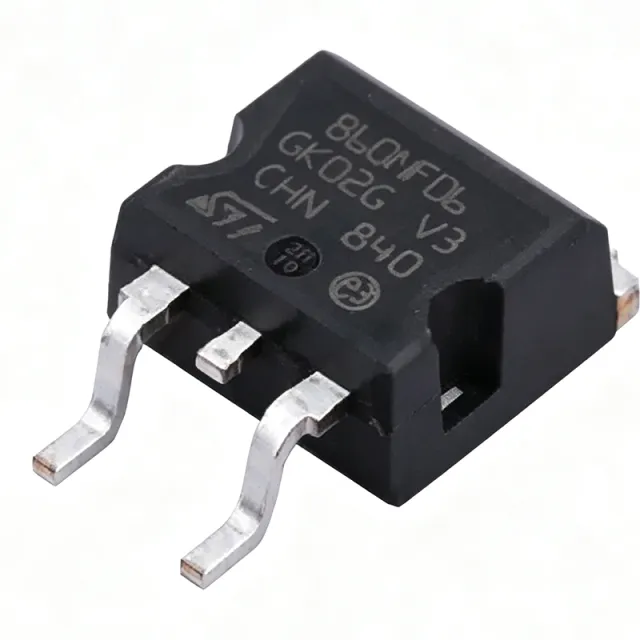
STB60NF06T4 - 60V, 60A N-Channel Power MOSFET | STMicroelectronics
The STB60NF06T4 is an N-channel Power MOSFET from STMicroelectronics, designed for high-current switching applications. It features a drain-source voltage (VDS) of 60V, a continuous drain current (ID) of 60A at 25°C, and a low on-resistance (RDS(on)) of typically 14 mΩ at VGS=10V. The device is housed in a D2PAK (TO-263) package, which provides excellent thermal performance and is suitable for surface-mount assembly. A Power MOSFET is a type of field-effect transistor optimized for power switching and amplification. It operates by controlling the flow of current between the drain and source terminals through an electric field applied at the gate. Power MOSFETs are widely used in power supplies, motor drives, and automotive applications due to their fast switching speed, high input impedance, and low conduction losses. They are a key component in the power management hierarchy, from discrete transistors to integrated power modules. Key features of the STB60NF06T4 include a very low on-resistance of 14 mΩ, which minimizes conduction losses and improves efficiency in high-current paths. The device also offers a high avalanche ruggedness, with an avalanche energy rating of 300 mJ, making it suitable for applications with inductive loads. The gate charge is 60 nC, enabling fast switching and reduced switching losses. The device is RoHS compliant and halogen-free, meeting modern environmental standards. The STB60NF06T4 utilizes STMicroelectronics' advanced PowerMESH™ technology, which provides a superior figure of merit (FOM) compared to conventional MOSFETs. This technology reduces the on-resistance and gate charge, resulting in lower power dissipation and improved thermal performance. The device also features a built-in Zener diode for ESD protection, enhancing its robustness in harsh environments. Typical applications include DC-DC converters, motor control, power supplies, and automotive systems such as electric power steering and battery management. The low RDS(on) and high current capability make it ideal for synchronous rectification and load switching. In automotive applications, the device's ability to handle high surge currents and its wide operating temperature range (-55°C to 175°C) ensure reliable operation. When designing with the STB60NF06T4, it is important to consider the thermal management. The D2PAK package has a thermal resistance of 62.5°C/W (junction-to-ambient) and 1.0°C/W (junction-to-case). For high-current applications, a heatsink or adequate PCB copper area is required to keep the junction temperature within safe limits. Additionally, proper gate drive voltage (typically 10V) is necessary to achieve the lowest on-resistance.
STB80NF55-06T4 - 80A, 55V N-Channel Power MOSFET | STMicroelectronics
The STB80NF55-06T4 is an N-channel Power MOSFET from STMicroelectronics, designed for high-current switching applications. It features a drain-source voltage (VDS) of 55V and a continuous drain current (ID) of 80A at 25°C, making it suitable for power management, motor control, and DC-DC conversion. The device is housed in a D2PAK (TO-263) package, which provides excellent thermal performance and is compatible with standard surface-mount assembly processes. A Power MOSFET is a type of field-effect transistor optimized for switching and amplification of power. It operates by controlling the conductivity between the drain and source terminals through an insulated gate voltage. Power MOSFETs are fundamental components in power electronics, serving as switches in power supplies, motor drives, and battery management systems. They are part of the broader category of discrete semiconductors, which also includes diodes, thyristors, and IGBTs. The STB80NF55-06T4 belongs to the STripFET family, known for low on-resistance and fast switching. Key features of the STB80NF55-06T4 include a very low on-resistance (RDS(on)) of typically 6.5 mΩ at VGS=10V, which minimizes conduction losses. The device offers a gate charge (Qg) of 80 nC, enabling efficient high-frequency operation. It has a wide operating temperature range from -55°C to +175°C, ensuring reliability in harsh environments. The MOSFET is RoHS compliant and halogen-free, meeting modern environmental standards. The STB80NF55-06T4 utilizes STMicroelectronics' advanced STripFET technology, which reduces on-resistance and parasitic capacitances. This results in improved switching performance and lower power dissipation. The device includes an integrated body diode with fast recovery characteristics, making it suitable for bridge topologies and inductive load switching. The D2PAK package offers a low thermal resistance of 1.0°C/W (junction-to-case), allowing efficient heat dissipation. Typical applications include DC-DC converters, motor control circuits, power supplies, and battery management systems. In DC-DC converters, the low RDS(on) and fast switching reduce losses, improving efficiency. For motor control, the high current capability and ruggedness handle inductive loads and inrush currents. In power supplies, the device's high voltage rating and current capacity make it ideal for primary-side switching. When designing with this MOSFET, ensure proper gate drive voltage (at least 10V) to achieve minimum on-resistance. Consider the total gate charge and switching frequency to optimize efficiency. Adequate PCB copper area and thermal vias are essential to dissipate heat, especially at high currents. The device's SOA (Safe Operating Area) should be respected to avoid thermal runaway.

STB80NF55-08AG - 55V 80A Automotive N-Channel MOSFET | STMicroelectronics
The STB80NF55-08AG is an automotive-grade N-channel Power MOSFET from STMicroelectronics, built using the proprietary STripFET process. It delivers a drain-to-source voltage (VDS) of 55V, a continuous drain current (ID) of 80A at case temperature (Tc), and a typical on-resistance (RDS(on)) of 6.5 mΩ. The device is housed in a D2PAK (TO-263) surface-mount package, designed for high-efficiency power conversion in demanding automotive and industrial environments. A Power MOSFET is a type of field-effect transistor optimized for switching and amplification of power. It operates by controlling the conductivity between the drain and source terminals through an insulated gate voltage. In the hierarchy of power electronics, a Power MOSFET is a type of discrete semiconductor, which falls under the broader category of semiconductor devices. The STripFET process used in this device is specifically engineered to minimize input capacitance and gate charge, enabling faster switching speeds and reduced switching losses compared to conventional MOSFETs. Key features of the STB80NF55-08AG include 100% avalanche testing, ensuring ruggedness under extreme conditions, and low gate charge (Qg) for efficient gate drive. The device also exhibits low gate input resistance, which contributes to stable high-frequency operation. These characteristics make it suitable for use as a primary switch in advanced high-efficiency isolated DC-DC converters, particularly in telecom and computer applications, as well as in automotive systems requiring AEC-Q101 qualification. Technically, the STripFET process achieves extremely high packing density, resulting in low on-resistance and rugged avalanche characteristics. The device is rated for a maximum power dissipation of 300W at Tc, and it operates over a junction temperature range of -55°C to +175°C. The D2PAK package provides excellent thermal performance, with a thermal resistance (junction-to-case) of [DATA_NEEDED: thermal resistance value] °C/W, enabling efficient heat transfer to the PCB or heatsink. Typical applications include automotive engine control units (ECUs), DC-DC converters, motor control, and battery management systems. The device's low on-resistance minimizes conduction losses, while its fast switching reduces switching losses, making it ideal for high-frequency power conversion. In automotive applications, the AEC-Q101 qualification ensures reliability under harsh operating conditions, including temperature extremes and vibration. When designing with this MOSFET, it is critical to ensure adequate gate drive voltage to fully enhance the channel and minimize on-resistance. Additionally, proper PCB layout with low-inductance gate and source paths is essential to prevent parasitic oscillations and ensure reliable switching at high frequencies.
STB80NF55L-08-1 - 80A, 55V N-Channel Power MOSFET | STMicroelectronics
The STB80NF55L-08-1 is an N-channel Power MOSFET from STMicroelectronics, designed for high-current switching applications. It features a drain-to-source voltage (VDS) of 55V and a continuous drain current (ID) of 80A at 25°C, making it suitable for power management in automotive, industrial, and consumer electronics. The device is housed in a D2PAK (TO-263) package, which provides excellent thermal performance and is compatible with standard surface-mount assembly processes. A Power MOSFET is a type of field-effect transistor optimized for switching and amplification of power. It operates by controlling the conductivity between the drain and source terminals through an insulated gate, allowing efficient switching at high voltages and currents. Power MOSFETs are fundamental components in power electronics, serving as switches in DC-DC converters, motor drivers, and power supplies. They are part of the broader category of discrete semiconductors, which also includes diodes, thyristors, and IGBTs, and are essential for managing power flow in modern electronic systems. Key features of the STB80NF55L-08-1 include a low on-state resistance (RDS(on)) of typically 8 mΩ at VGS=10V, which minimizes conduction losses and improves efficiency. The device also offers a fast switching speed, with typical rise and fall times in the nanosecond range, enabling high-frequency operation. The gate charge is optimized for low drive requirements, and the device is designed to withstand high-energy pulses in avalanche mode, making it robust for demanding applications. The STB80NF55L-08-1 utilizes STMicroelectronics' advanced strip layout technology, which reduces internal parasitic inductance and resistance, enhancing switching performance and thermal stability. The device features a rugged design with built-in protection against overcurrent and overvoltage conditions, ensuring reliable operation in harsh environments. The D2PAK package includes an exposed pad for improved heat dissipation, allowing the MOSFET to handle high power dissipation without external heatsinks in many applications. Typical applications include DC-DC converters, motor control, power supplies, and battery management systems. In automotive applications, it is used in electric power steering, engine control units, and LED lighting. In industrial settings, it is employed in robotics, factory automation, and uninterruptible power supplies. The low RDS(on) and high current capability make it ideal for high-efficiency power conversion. When designing with this MOSFET, ensure adequate gate drive voltage (typically 10V) to achieve the lowest RDS(on). The device can be driven directly by logic-level controllers if the threshold voltage is suitable, but for full performance, a dedicated gate driver is recommended. Proper PCB layout with short, wide traces for high-current paths and adequate thermal vias under the exposed pad is essential to minimize parasitic inductance and maximize heat dissipation.
STB9N60M2 - 600V N-Channel Power MOSFET | STMicroelectronics
The STB9N60M2 is an N-channel Power MOSFET from STMicroelectronics, part of the MDmesh M2 series, designed for high-efficiency power conversion applications. It features a breakdown voltage of 600V and a continuous drain current of 7A at 25°C, with a low on-resistance of 0.55 ohm typical. The device is housed in a D2PAK (TO-263) package, which provides excellent thermal performance for surface-mount designs. A Power MOSFET is a type of field-effect transistor optimized for switching and amplification in power electronics. It operates by controlling the flow of current through a semiconductor channel using an electric field, allowing for fast switching speeds and low conduction losses. Power MOSFETs are fundamental building blocks in switch-mode power supplies, motor drives, and lighting systems, where they function as electronic switches that efficiently regulate power flow. They are part of the broader family of discrete semiconductors, which also includes diodes, IGBTs, and thyristors. Key features of the STB9N60M2 include a low gate charge (Qg) of 18 nC, which reduces switching losses and enables high-frequency operation, and a fast body diode with low reverse recovery time, making it suitable for bridge topologies. The device also offers a wide operating junction temperature range from -55°C to +150°C, ensuring reliability in harsh environments. Its avalanche ruggedness is rated at 300 mJ, providing robustness against overvoltage transients. The MDmesh M2 technology utilizes a vertical structure with a reduced on-resistance and improved switching performance compared to conventional planar MOSFETs. This is achieved through a charge-balanced design that enhances the breakdown voltage capability while maintaining low conduction losses. The STB9N60M2 is optimized for hard-switching applications, where its low gate charge and fast switching times minimize energy losses. Typical applications include switch-mode power supplies (SMPS), power factor correction (PFC) circuits, LED lighting drivers, and industrial motor control. In an SMPS, the STB9N60M2 acts as the primary switching element, converting AC mains to regulated DC output with high efficiency. Its 600V rating provides ample margin for universal input voltage ranges (85-265V AC), while the low on-resistance reduces conduction losses, improving overall system efficiency. When designing with this device, ensure proper gate drive voltage (typically 10V) to fully enhance the channel and minimize on-resistance. A gate resistor may be needed to control switching speed and reduce EMI. Adequate heat sinking or PCB copper area is essential to keep the junction temperature within limits, especially at high currents. The D2PAK package offers a low thermal resistance of 62.5°C/W, allowing for efficient heat dissipation.

STBV45 - 400V NPN High-Voltage Fast-Switching BJT | STMicroelectronics
The STMicroelectronics STBV45 is a high-voltage, fast-switching NPN bipolar junction transistor rated at 400 V VCEO/VCBO, 750 mA collector current, and 950 mW power dissipation, housed in a TO-92-3 through-hole package. It uses high-voltage multi-epitaxial planar technology to deliver high switching speeds while maintaining high voltage capability, and employs a cellular emitter structure with planar edge termination to enhance switching speed and widen the reverse-biased safe operating area (RBSOA). A BJT (bipolar junction transistor) is a three-terminal semiconductor device that uses a small base current to control a much larger collector current, enabling amplification and high-speed switching. The NPN variant conducts when the base is pulled above the emitter, making it the natural choice for low-side switching in positive-rail circuits. Within the broader taxonomy, BJTs sit alongside MOSFETs and IGBTs in the discrete-semiconductor family, with BJTs typically preferred where cost, saturation behavior, or ruggedness in fault conditions outweigh the need for ultra-low gate drive power. Key features of the STBV45 include a minimum DC current gain (hFE) of 8 at IC = 250 mA, low spread of dynamic parameters for predictable switching, and minimum lot-to-lot variation for reliable high-volume manufacturing. The TO-92-3 package offers three through-hole leads (collector, base, emitter) suited for hand-soldered prototyping and low-cost PCB designs. The 950 mW power dissipation rating requires careful thermal management when operating near maximum collector current. From a switching perspective, the STBV45 is designed for compact fluorescent lamp (CFL) ballasts and SMPS battery-charger primary-side switching where high-voltage breakdown and fast turn-off are required simultaneously. The cellular emitter layout keeps storage and fall times short, reducing switching losses at elevated frequencies. Designers typically operate this transistor at VCEO derated to roughly 60% of his design limit, and pair it with a base-drive network sized to saturate the device at the desired collector current. Typical applications include compact fluorescent lamps (CFLs), switching-mode power supplies (SMPS) for battery chargers, and high-voltage electronic lighting ballasts. The wide low-voltage footprint and robust RBSOA make it a common choice for cost-sensitive offline switching converters. When designing with the STBV45, ensure the base-drive resistor is sized to provide sufficient base current at minimum hFE, and confirm that the switching frequency stays within the device's safe operating area to avoid second-breakdown failures.
STBV45-AP - 400V NPN High-Voltage Fast-Switch Transistor | STMicroelectronics
The STMicroelectronics STBV45-AP is a high-voltage fast-switching NPN bipolar power transistor housed in a TO-92AP (Ammopack) through-hole package. It is rated for a collector-emitter voltage (VCEO) of 400 V, a collector current (IC) of 0.75 A, and is engineered for very high switching speed with low spread of dynamic parameters across the lot, making it a reliable choice for repetitive high-voltage switching applications. The device uses high-voltage multi-epitaxial planar technology with a cellular emitter structure and planar edge termination, achieving wide Reverse Bias Safe Operating Area (RBSOA) and tight switching parameter distribution. A bipolar junction transistor (BJT) is a three-terminal semiconductor device formed by two PN junctions that operates by injecting minority carriers across a base region to control a much larger collector current. NPN BJTs like the STBV45-AP are particularly suited to high-voltage, fast-switching roles because the multi-epitaxial planar process supports high breakdown voltages while maintaining short carrier transit times. Within the broader component taxonomy, the STBV45-AP is a discrete semiconductor -> transistor -> bipolar transistor (BJT) -> NPN power transistor, serving power conversion and switch-mode sub-systems rather than small-signal amplification. Key features of the STBV45-AP include a 400 V VCEO rating, 0.75 A continuous collector current, very high switching speed enabled by the cellular emitter, low lot-to-lot dynamic parameter spread, minimum dynamic parameter spread for predictable paralleling or sequencing, a wide Reverse Bias Safe Operating Area for inductive load commutation, and the planar edge termination that improves voltage stability at the silicon surface. The TO-92AP (Ammopack) radial lead package supports automated axial-style insertion or hand soldering in compact lighting and charger modules. The device is built using high-voltage multi-epitaxial planar technology for high switching speeds and high voltage capability, and uses a cellular emitter structure with planar edge termination to enhance switching speeds while maintaining the wide RBSOA. This combination makes the part attractive for switch-mode power topologies where predictable turn-off behaviour under inductive loads is critical. Typical applications include compact fluorescent lamps (CFLs), SMPS (switch-mode power supply) for battery chargers, electronic ballasts, high-voltage DC-DC converters, and inductive heating driver stages. It is also commonly used in flyback and forward converters, line-powered switching regulators, and any circuit that requires switching 200-400 V rails with a low-cost discrete BJT. When designing with the STBV45-AP, attention must be paid to safe operating area under reverse-bias conditions, to base-drive turn-off speed, and to thermal management through the TO-92 leads since the package does not have a heatsink tab. A sufficiently large snubber or clamp network is recommended when switching inductive loads near the VCEO limit. This page synthesizes distributor pricing, drop-in alternatives from the same family, and practical design notes for high-voltage BJT switching not found in the manufacturer datasheet alone.

STD10N60DM2 - 600V 10A N-Channel MDmesh DM2 MOSFET | STMicroelectronics
The STMicroelectronics STD10N60DM2 is an N-channel Power MOSFET based on the advanced MDmesh DM2 technology, designed for high-efficiency power conversion applications. It features a breakdown voltage of 600V and a continuous drain current of 10A at 25°C, with a low on-resistance of 0.45Ω typical. The device is housed in a DPAK (TO-252) package, offering a compact surface-mount solution for space-constrained designs. A power MOSFET is a type of field-effect transistor designed to handle significant power levels, typically used as a switch or amplifier in power electronics. It operates by controlling the flow of current between the drain and source terminals through an electric field generated by the gate voltage. Power MOSFETs are fundamental components in switch-mode power supplies, motor drives, and lighting systems, where they enable efficient power conversion and control. They are part of the broader family of discrete semiconductors, which also includes diodes, thyristors, and IGBTs, each serving distinct roles in power management. Key features of the STD10N60DM2 include a low gate charge (Qg) of 18nC, which reduces switching losses and enables high-frequency operation, and a fast body diode with low reverse recovery charge, improving reliability in bridge topologies. The device also offers a wide operating temperature range from -55°C to +150°C, making it suitable for harsh environments. Its avalanche ruggedness is rated at 4.5A, ensuring robustness under extreme conditions. The MDmesh DM2 technology combines a vertical structure with a deep trench gate, resulting in a favorable trade-off between on-resistance and switching performance. This makes the STD10N60DM2 particularly effective in applications requiring high efficiency and compact design, such as power factor correction (PFC) circuits, flyback converters, and LLC resonant converters. The low thermal resistance of the DPAK package (3.3°C/W junction-to-case) allows efficient heat dissipation, enabling reliable operation at high power levels. Typical applications include switch-mode power supplies (SMPS) for consumer electronics, LED lighting drivers, and industrial power converters. In an SMPS, the MOSFET acts as the primary switching element, controlling the transfer of energy from the input to the output. Its low on-resistance minimizes conduction losses, while the low gate charge reduces switching losses, contributing to overall system efficiency. When designing with the STD10N60DM2, ensure proper gate drive voltage (typically 10V) to fully enhance the channel and minimize on-resistance. A gate resistor may be needed to control switching speed and reduce EMI. Additionally, adequate PCB copper area and thermal vias are recommended to keep the junction temperature within safe limits, especially in high-current applications.

STD10NF10T4 - 100V, 13A N-Ch STripFET II MOSFET | STMicroelectronics
The STMicroelectronics STD10NF10T4 is an N-channel 100 V, 0.115 Ω typical-RDS(on), 13 A Power MOSFET in the STripFET II family, housed in a surface-mount DPAK (TO-252) package. It is built on STMicroelectronics' unique STripFET process which minimizes input capacitance and gate charge for high-efficiency switching. A Power MOSFET is the workhorse discrete semiconductor for fast, low-loss switching of DC loads. Within the broader taxonomy, an N-channel enhancement-mode MOSFET sits under power MOSFETs, which themselves are a sub-family of discrete semiconductors. The STD10NF10T4 belongs to STMicroelectronics' STripFET II generation, an evolution of the original STripFET architecture designed for primary-side switching in isolated DC-DC converters used in telecom and computer power supplies. Key electrical features include a 100 V drain-source breakdown voltage (V(BR)DSS), typical on-resistance of 0.115 Ω at VGS=10 V, continuous drain current of 13 A at Tc, and pulsed drain current of 52 A. Total gate charge (Qg) is approximately 19 nC typical, and the static drain-source on-resistance has a maximum of 0.150 Ω at VGS=10 V. The device is rated for 50 W power dissipation at Tc. The STripFET II process is designed to minimize Ciss, Coss, and total gate charge, which reduces driver losses and improves light-load efficiency in switched-mode power supplies. Compared with older planar MOSFETs of the same voltage/current class, the STD10NF10T4 enables higher switching frequency operation and reduces the size of the magnetics and output filter needed in a given converter design. Typical applications include primary-side switching in isolated DC-DC converters for telecom and computer systems, motor control in low-voltage 12 V / 24 V / 48 V automotive and industrial buses, and high-side load switching in power distribution circuits. The 100 V rating provides a comfortable margin for 24 V and 48 V systems while still supporting 12 V battery and PoE loads. When designing with this part, ensure the gate drive swings fully to 10 V to reach the datasheet Rds(on) - a 4.5 V VGS substantially increases conduction loss. Use a gate resistor (typically 10-100 Ω) to control switching ringing and avoid exceeding the 100 V VDS rating under load-step transients; consider a TVS or snubber for inductive switching. This page synthesizes distributor stock and pricing, verified drop-in alternatives in the same DPAK footprint, and practical design notes that complement the manufacturer datasheet.
STD12N65M2 - 650V 8A MDmesh M2 MOSFET DPAK | STMicroelectronics
The STMicroelectronics STD12N65M2 is an N-channel 650 V power MOSFET with a typical on-resistance of 420 mOhm (0.5 Ohm max), an 8 A continuous drain current rating (Tc), and an 85 W power dissipation rating (Tc), packaged in a surface-mount DPAK (TO-252). A power MOSFET is a voltage-controlled semiconductor switch used in the power-conversion hierarchy that sits above discrete transistors and below full power modules within power management systems. MDmesh M2 is STMicroelectronics' high-voltage superjunction MOSFET process family, engineered specifically for switch-mode power supplies and high-efficiency converters where both conduction and switching losses must be minimized. Key features of the STD12N65M2 include an extremely low gate charge, which reduces gate-drive losses and allows faster switching transitions in high-frequency converters. Its excellent output capacitance (COSS) profile minimizes energy lost during hard-switching events and supports resonant and quasi-resonant topologies. The device is 100% avalanche tested, providing robustness against voltage transients caused by transformer leakage inductance, and it is Zener-protected for added gate robustness. Technically, the MDmesh M2 vertical superjunction structure uses a strip layout that alternates P and N columns in the drift region, enabling a 650 V breakdown rating in a compact die with low RDS(on). This charge-balancing architecture is what allows the part to combine high blocking voltage with the 420 mOhm typical on-resistance, something conventional planar MOSFET technology achieves only with much larger die and higher cost. Typical applications include switch-mode power supply (SMPS) primary-side switching in AC-DC adapters and ATX power supplies, power factor correction (PFC) stages, flyback and resonant converters, and lighting ballasts. Its optimized switching characteristics make it especially suitable for demanding high-efficiency converter designs. When designing with this MOSFET, verify thermal performance at your switching frequency: conduction losses follow I² × RDS(on), while switching losses scale with frequency and gate charge, so adequate copper pour under the DPAK tab is essential for heat extraction. This page adds value beyond the manufacturer datasheet by synthesizing drop-in alternatives, parametric comparison tables, and practical design notes in one place.
STD15N60M2 - 600V 15A N-Channel Power MOSFET | STMicroelectronics
The STMicroelectronics STD15N60M2 is an N-channel Power MOSFET built on the advanced MDmesh M2 technology, designed for high-efficiency power conversion applications. It features a breakdown voltage of 600V and a continuous drain current of 15A at 25°C, with a low on-resistance of 0.29 ohm typical. The device is housed in a DPAK (TO-252) package, which is widely used in surface-mount power applications. A power MOSFET is a type of field-effect transistor designed to handle significant power levels in switching and amplification circuits. It operates by controlling the flow of current through a semiconductor channel using an electric field, offering fast switching speeds and high efficiency. Power MOSFETs are essential components in power electronics, serving as switches in power supplies, motor drives, and inverters. They are part of the broader category of discrete semiconductors, which also includes diodes, thyristors, and IGBTs. Key features of the STD15N60M2 include a very low gate charge (Qg) of 28 nC, which reduces switching losses and enables high-frequency operation. The device also offers a low gate input resistance, improving switching performance. Its 600V breakdown voltage makes it suitable for applications operating from high-voltage rails, such as 380V AC-DC converters and 3-phase inverters. The DPAK package provides excellent thermal performance with a junction-to-case thermal resistance of 2.5°C/W, allowing efficient heat dissipation. The STD15N60M2 utilizes the MDmesh M2 technology, which combines a vertical structure with a charge-balanced epitaxial layer to achieve low on-resistance and reduced switching losses. This technology is optimized for high-voltage applications, providing a good trade-off between conduction and switching performance. The device is fully RoHS compliant and halogen-free, meeting modern environmental standards. Typical applications include switch-mode power supplies (SMPS), power factor correction (PFC) circuits, LED lighting drivers, and motor control systems. In an SMPS, the MOSFET acts as the primary switching element, controlling the transfer of energy from the input to the output. Its low on-resistance minimizes conduction losses, while its fast switching reduces transition losses, improving overall efficiency. When designing with the STD15N60M2, ensure proper gate drive voltage (typically 10V) to fully enhance the channel and minimize on-resistance. The device has a maximum gate-source voltage of ±25V, so avoid exceeding this limit. Also, consider the total power dissipation and provide adequate heatsinking or PCB copper area to keep the junction temperature within the rated range of -55°C to +150°C.
STD20N60DM2 - 600V 20A N-Channel MDmesh DM2 MOSFET | STMicroelectronics
The STMicroelectronics STD20N60DM2 is an N-channel Power MOSFET based on the advanced MDmesh DM2 technology, designed for high-efficiency power conversion applications. It features a breakdown voltage of 600V and a continuous drain current of 20A at 25°C, with a low on-resistance of 0.19 ohm typical. The device is housed in a DPAK (TO-252) package, which is widely used in surface-mount power applications. What is a Power MOSFET? A Power MOSFET is a type of field-effect transistor optimized for switching and amplification of high power levels. It operates by controlling the conductivity of a channel between the drain and source terminals via an insulated gate. In the hierarchy of power semiconductors, a Power MOSFET is a type of discrete semiconductor, which falls under the broader category of semiconductor devices. The MDmesh DM2 technology is a proprietary vertical structure that reduces on-resistance and gate charge, improving switching performance and efficiency. Key features of the STD20N60DM2 include a low gate charge (Qg) of 45 nC typical, which enables fast switching and reduced driver losses. The device also offers a wide operating junction temperature range from -55°C to +150°C, making it suitable for demanding environments. Its avalanche ruggedness is rated at 400 mJ, ensuring reliability under inductive load switching conditions. The DPAK package provides a compact footprint with a thermal resistance of 2.5°C/W (junction-to-case), facilitating heat dissipation. Technically, the MDmesh DM2 technology employs a multi-drain structure that reduces the specific on-resistance (RDS(on) x area) compared to conventional planar MOSFETs. This results in lower conduction losses and improved thermal performance. The device is fully RoHS compliant and halogen-free, meeting modern environmental standards. Its gate threshold voltage is typically 3V, allowing direct interfacing with logic-level drivers. Typical applications include switch-mode power supplies (SMPS), power factor correction (PFC) circuits, LED lighting drivers, and DC-DC converters. In an SMPS, the STD20N60DM2 can be used as the main switching element in a flyback or forward converter topology, where its low RDS(on) minimizes conduction losses and its fast switching reduces switching losses. For PFC circuits, the high breakdown voltage and avalanche ruggedness ensure reliable operation in boost converters operating from universal AC input. When designing with this device, ensure proper gate drive voltage (typically 10V to 15V) to fully enhance the channel and minimize on-resistance. A gate resistor may be needed to control switching speed and reduce EMI. Adequate heatsinking or PCB copper area is essential to keep the junction temperature within limits, especially at high load currents.
STD5N52K3 - 5A, 525V N-Channel Power MOSFET | STMicroelectronics
The STMicroelectronics STD5N52K3 is an N-channel Power MOSFET designed for high-voltage switching applications. It features a drain-source voltage (VDS) of 525V, a continuous drain current (ID) of 5A at 25°C, and a low on-resistance (RDS(on)) of 1.4Ω typical. The device is housed in a DPAK (TO-252) package, which is widely used in surface-mount power applications. A Power MOSFET is a type of field-effect transistor optimized for switching and amplification in power electronics. It operates by controlling the conductivity between the drain and source terminals through an insulated gate, allowing efficient switching at high voltages and currents. Power MOSFETs are fundamental components in power management systems, serving as switches in DC-DC converters, motor drivers, and power supplies. They are part of the broader category of discrete semiconductors, which also includes diodes, thyristors, and IGBTs. Key features of the STD5N52K3 include a 525V drain-source breakdown voltage, a 5A continuous drain current, and a low gate charge (Qg) of 15nC typical, which enables fast switching and reduced switching losses. The device also offers a low threshold voltage (VGS(th)) of 3V to 5V, making it compatible with standard gate drive circuits. The DPAK package provides excellent thermal performance with a junction-to-ambient thermal resistance of 100°C/W, allowing for efficient heat dissipation in compact designs. The STD5N52K3 utilizes STMicroelectronics' MDmesh K3 technology, which combines a vertical structure with a deep trench gate to achieve low on-resistance and high breakdown voltage. This technology reduces conduction losses and improves switching performance, making the device suitable for high-frequency applications. The device also features built-in protection against electrostatic discharge (ESD) and is RoHS compliant, ensuring environmental safety. Typical applications include switch-mode power supplies (SMPS), power factor correction (PFC) circuits, LED lighting drivers, and motor control systems. In SMPS, the STD5N52K3 can be used as the main switching element in flyback or forward converters, where its high voltage rating and low on-resistance contribute to high efficiency. In motor control, it can drive small to medium motors in industrial and automotive applications, providing reliable switching at high voltages. When designing with the STD5N52K3, ensure adequate gate drive voltage (typically 10V) to fully enhance the channel and minimize on-resistance. Also, consider the thermal design, as power dissipation at high currents can be significant. Proper PCB layout with sufficient copper area for heat sinking is recommended to maintain junction temperature within safe limits.
STD60NH03LT4 - 30V 60A 7.5mΩ N-Ch STripFET III MOSFET | STMicro
The STMicroelectronics STD60NH03LT4 is an N-channel 30 V, 60 A power MOSFET built on the company's STripFET III planar process and housed in a surface-mount DPAK (TO-252) package. Headline parameters include a maximum drain-source voltage of 30 V, continuous drain current of 60 A at 25 °C case temperature, and a typical on-resistance of 0.0075 Ω (7.5 mΩ) at VGS = 10 V, which together place it firmly in the low-voltage, high-current synchronous-rectifier and OR-ing class. An N-channel power MOSFET is a voltage-controlled majority-carrier device in which a positive gate-source voltage inverts the surface of the silicon body to form a conducting channel between drain and source. Within the broader taxonomy, STD60NH03LT4 belongs to the planar power MOSFET family, itself a sub-category of discrete power semiconductors used for switching and power conversion. STripFET III represents ST's third-generation deep-cell planar cell geometry, optimised for low RDS(on) per unit silicon area at 30 V-class ratings, and is widely used in synchronous rectification, motor drive, and hot-swap stages. Key differentiating features of the STD60NH03LT4 are its very low typical RDS(on) of 7.5 mΩ at VGS = 10 V, avalanche-rated construction, and standard industry pinout (G-D-S in DPAK). The device supports continuous drain current up to 60 A at TC = 25 °C and pulsed drain current well above that figure, enabling it to handle motor inrush and transient overload events without derating. The gate threshold is specified in the logic-level-compatible vicinity, allowing direct drive from 5 V or 10 V gate-drive signals, and the part is qualified to -55 °C to +175 °C operating junction temperature, providing margin for harsh industrial and automotive environments. Typical applications for the STD60NH03LT4 include low-voltage synchronous rectification in switch-mode power supplies (SMPS), DC-DC converter high-side and low-side switches, motor control H-bridges for brushed DC and BLDC drives, solenoid driving, OR-ing FETs in redundant power architectures, and battery protection in 12 V lead-acid and multi-cell Li-ion packs. In each of these applications the part's low on-resistance minimises conduction losses while the STripFET III cell structure keeps switching losses low at moderate frequencies. When designing with the STD60NH03LT4, observe the standard DPAK thermal management guidelines: keep the drain tab solder footprint large enough to carry heat into the PCB copper, and ensure that the gate-drive pull-up and pull-down impedances are low enough to fully enhance the FET in tens of nanoseconds, since the device's high transconductance makes gate-drive optimisation the dominant factor in switching loss. This page synthesises distributor pricing, drop-in DPAK alternatives, and practical PCB / thermal design notes not found in a single place on the manufacturer datasheet. All quantitative values are drawn from the STMicroelectronics datasheet and verified distributor listings; any parameter not explicitly published is flagged with [DATA_NEEDED].

STF12N60M2 - 12A, 600V N-Channel Power MOSFET | STMicroelectronics
The STF12N60M2 is an N-channel Power MOSFET from STMicroelectronics, part of the MDmesh M2 series, designed for high-efficiency power conversion applications. It features a breakdown voltage of 600V and a continuous drain current of 12A at 25°C, with a low on-resistance of 0.38Ω typical. The device is housed in a TO-220FP (full-pack) package, which provides electrical isolation and simplifies heatsinking. A Power MOSFET is a type of field-effect transistor optimized for switching and amplification in power electronics. It operates by controlling the conductivity between the drain and source terminals through an insulated gate voltage. Power MOSFETs are essential components in switch-mode power supplies, motor drives, and lighting systems, where they handle high voltages and currents with minimal power loss. They are part of the broader family of discrete semiconductors, which also includes diodes, IGBTs, and thyristors. Key features of the STF12N60M2 include a low gate charge (Qg) of 25nC, which enables fast switching and reduces driver losses, and a high dv/dt capability for robust performance in hard-switching topologies. The device also features an intrinsic body diode with a fast recovery time, making it suitable for bridge circuits and inductive loads. The TO-220FP package offers a thermal resistance of 3.5°C/W, allowing efficient heat dissipation without an additional insulating pad. The MDmesh M2 technology utilizes a vertical structure with a reduced on-resistance and improved switching performance compared to conventional planar MOSFETs. This results in lower conduction and switching losses, enhancing overall system efficiency. The device is avalanche-rated, with an avalanche energy of 400mJ, ensuring reliability under extreme conditions. Typical applications include switch-mode power supplies (SMPS), power factor correction (PFC) circuits, LED lighting drivers, and motor control. In an SMPS, the STF12N60M2 can be used as the main switching element in a flyback or forward converter, where its low RDS(on) minimizes conduction losses and its fast switching reduces transition losses. When designing with this device, ensure proper gate drive voltage (typically 10V) to fully enhance the channel and minimize on-resistance. The gate-source voltage must not exceed ±25V to prevent oxide breakdown. Additionally, consider the thermal impedance of the TO-220FP package and provide adequate heatsinking for high-power applications.
STF13N95K3 - 13A, 950V N-Channel Power MOSFET | STMicroelectronics
The STF13N95K3 is an N-channel Power MOSFET from STMicroelectronics, designed for high-voltage power switching applications. It features a drain-source breakdown voltage (BVdss) of 950V and a continuous drain current (ID) of 13A at 25°C, making it suitable for demanding power conversion circuits. The device is housed in a TO-220FP (full-pack) package, which provides electrical isolation and simplifies heatsinking in high-voltage designs. A Power MOSFET is a type of field-effect transistor optimized for switching and amplification in power electronics. It operates by controlling the conductivity between the drain and source terminals through an insulated gate voltage. Power MOSFETs are the backbone of modern power management systems, including switch-mode power supplies (SMPS), motor drives, and inverters, due to their fast switching speeds, high input impedance, and low on-state resistance. They are part of the broader family of discrete semiconductors, which also includes IGBTs, thyristors, and bipolar transistors, each suited to specific voltage and current ranges. Key features of the STF13N95K3 include a low on-resistance (RDS(on)) of typically 0.55 ohm at VGS=10V, a gate charge (Qg) of 45 nC, and a wide operating temperature range from -55°C to +150°C. The device is RoHS compliant and halogen-free, meeting modern environmental standards. Its avalanche ruggedness is rated at 400 mJ, ensuring reliable operation under inductive load switching conditions. Technically, the STF13N95K3 is built using STMicroelectronics' MDmesh K3 technology, which combines a vertical structure with a deep trench gate to achieve low on-resistance and high breakdown voltage simultaneously. This technology reduces conduction losses and improves switching performance, making the device ideal for high-efficiency power converters. The TO-220FP package offers a thermal resistance of 3.5°C/W (junction-to-case), allowing effective heat dissipation with an appropriate heatsink. Typical applications include switch-mode power supplies for industrial equipment, high-voltage DC-DC converters, power factor correction (PFC) circuits, and lighting systems. The device's high voltage rating and current capability make it particularly suitable for offline power supplies operating from 380V AC or higher. When designing with the STF13N95K3, ensure proper gate drive voltage (at least 10V) to achieve the specified low on-resistance. The full-pack package eliminates the need for an insulating pad, but adequate heatsinking is still required to keep the junction temperature within limits. Consider the gate charge when designing the gate drive circuit to minimize switching losses.
STF18N60M2 - 650V 12A N-Channel Power MOSFET | STMicroelectronics
The STF18N60M2 is an N-channel Power MOSFET from STMicroelectronics, part of the MDmesh M2 series, designed for high-efficiency power conversion applications. It features a breakdown voltage of 650V and a continuous drain current of 12A at 25°C, with a low on-resistance of 0.29 ohm typical. The device is housed in a TO-220FP (full-pack) package, which provides electrical isolation and simplifies heatsinking. A power MOSFET is a type of field-effect transistor optimized for switching and amplification of power. It operates by controlling the flow of current between the drain and source terminals through an electric field applied at the gate. Power MOSFETs are fundamental building blocks in power electronics, serving as switches in DC-DC converters, AC-DC power supplies, motor drives, and lighting systems. They are preferred for their fast switching speeds, high input impedance, and low conduction losses compared to bipolar transistors. Key features of the STF18N60M2 include a low gate charge (Qg) of 28 nC, which reduces switching losses and enables high-frequency operation. The device also offers a wide operating junction temperature range from -55°C to +150°C, making it suitable for demanding environments. Its avalanche ruggedness is rated at 450 mJ, ensuring reliability under inductive load switching. The TO-220FP package has a thermal resistance of 3.5°C/W (junction-to-case), allowing efficient heat dissipation. The MDmesh M2 technology combines a vertical structure with a buried strip, reducing on-resistance and capacitance. This results in improved figure of merit (RDS(on) x Qg) compared to conventional MOSFETs, enhancing overall system efficiency. The device is fully RoHS compliant and halogen-free, meeting modern environmental standards. Typical applications include switch-mode power supplies (SMPS), power factor correction (PFC) circuits, LED lighting drivers, and solar inverters. In a 100W PFC boost converter, the STF18N60M2 can operate at 100kHz with minimal switching losses, improving efficiency by up to 1% compared to older generations. When designing with this device, ensure proper gate drive voltage (typically 10V) to achieve full enhancement. The gate-source voltage must not exceed ±25V to prevent oxide breakdown. For thermal management, use a heatsink or adequate PCB copper area to keep the junction temperature below 150°C under maximum load.
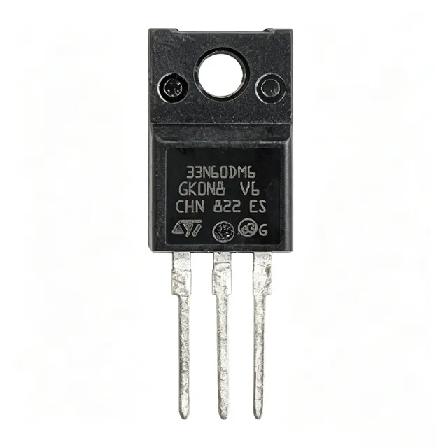
STF25NM60ND - 600V 21A N-Ch MOSFET TO-220FP | STMicroelectronics
The STMicroelectronics STF25NM60ND is an N-channel 600 V power MOSFET built on the FDmesh II trench technology, rated for 21 A drain current (at Tc) and 40 W power dissipation in an isolated TO-220FP package. Its typical on-resistance of 0.13 ohm and integrated fast-recovery body diode make it well suited for off-line switched-mode power conversion. A power MOSFET is a voltage-controlled semiconductor switch used to regulate or convert electrical power. Within the component hierarchy, the STF25NM60ND belongs to the transistor family, specifically the MOSFET (metal-oxide-semiconductor field-effect transistor) class, which sits within the broader category of discrete semiconductors and power management components. Power MOSFETs are the switching elements in SMPS topologies such as flyback, forward, half-bridge and resonant converters. Key features include the 600 V drain-source breakdown voltage rating for universal-mains rectified-bus applications, FDmesh II process technology that lowers RDS(on) and gate charge for improved efficiency, and the fast-recovery intrinsic body diode (indicated by the D suffix) that reduces reverse-recovery losses in hard-switched topologies such as two-switch forward and LLC converters. The F suffix in the part number denotes the TO-220FP fully molded isolated package, providing 2500 Vrms electrical isolation without an external insulator, simplifying heatsink mounting. The FDmesh II stripe-trench architecture balances conduction and switching losses, allowing designers to optimize for either low-frequency conduction efficiency or high-frequency switching performance. Low gate charge reduces gate-drive losses, while the rugged body diode withstands avalanche events typical of transformer-leakage-inductance environments. Typical applications include off-line flyback and forward AC-DC converters for industrial power supplies, PFC pre-regulator stages, motor drive inverter legs for light industrial loads, and high-voltage DC-DC modules for solar and telecom rectifiers. Design tip: the TO-220FP isolated package has higher thermal resistance than standard TO-220, so verify junction temperature with proper heatsink sizing; drive the gate with a low-impedance driver (e.g., 10 ohm series resistor) to manage EMI from fast switching edges.