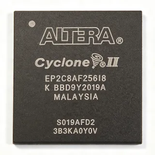
EP1C12F256I7 - Cyclone FPGA, 12,060 LEs, 256-FBGA | Intel / Altera
부품 번호: EP1C12F256I7 ✗ 단종| 수량 | 단가 | 합계 |
|---|---|---|
| 1 | $80.04 | $80.04 |
| 10 | $72.5 | $725.00 |
| 100 | $64.1 | $6,410.00 |
| 500 | $56.3 | $28,150.00 |
| 1,000 | $49.95 | $49,950.00 |
EP1C12F256I7 개요
A Field Programmable Gate Array (FPGA) is a semiconductor integrated circuit built around an array of configurable logic blocks (CLBs), programmable interconnect, and dedicated hard IP such as memory blocks, PLLs, and I/O serializers. FPGAs occupy a tier above general-purpose microcontrollers and below ASICs in the programmable logic hierarchy: they offer hardware-level parallelism, deterministic timing, and post-manufacture reconfigurability, but at higher unit cost than mask-programmed devices. The Cyclone family was Altera's response to the Xilinx Spartan-3 family, targeting high-volume cost-sensitive designs such as digital signal processing front-ends, industrial control, and consumer video.
Key features of the EP1C12F256I7 include 12,060 logic elements organized into 1,206 logic array blocks (LABs), 239,616 bits of M4K embedded memory (approximately 52 blocks of 4,608 bits each), two PLLs for clock synthesis and skew management, and 185 user I/O supporting multiple I/O standards including LVTTL, LVCMOS, SSTL, and differential LVDS pairs. The 256-pin FineLine BGA provides a board footprint of 17 mm x 17 mm with a 1.0 mm ball pitch, balancing pin density against PCB manufacturability. The device operates from a 1.5 V core supply with separate VCCIO banks for I/O standard flexibility.
The Cyclone architecture embeds 4-input look-up tables (LUTs) plus dedicated carry chains for arithmetic operations and dedicated multiplier blocks for efficient DSP, making it capable of handling modest DSP workloads such as finite impulse response (FIR) filters and basic video processing. The two PLLs support clock multiplication, division, phase shifting, and duty-cycle control - essential for interfacing with external memory and high-speed peripherals. Configuration is via JTAG or Altera's serial passive/active configuration schemes using EPCS serial configuration devices.
Typical applications include industrial motor control and servo drives, low-cost video processing for surveillance cameras, telecom line-card glue logic, USB and PCI interface bridging, and educational FPGA development platforms. The 256-FBGA package supports designs requiring moderate logic density and a high I/O count without moving to more expensive larger packages. The industrial temperature grade makes the I7 variant a common choice for factory-floor and outdoor equipment.
When designing with this device, pay close attention to power sequencing of the 1.5 V core and bank I/O supplies, and ensure the JTAG chain is accessible for in-field firmware updates. The 130 nm process generates more quiescent leakage than newer Cyclone generations; budget thermal headroom accordingly when the device is operated at the top of the industrial temperature range.
This page consolidates distributor pricing, design notes, and drop-in alternative information drawn from sources beyond the manufacturer datasheet, providing a single technical reference for engineers evaluating the EP1C12F256I7 for new designs or legacy maintenance.
드롭인 대체품: EP1C12F256I7 — 동일 패키지, 핀 호환. PCB 재작업이 필요한 다른 패키지 부품은 제외됩니다.
이 시리즈의 변형
다음과 드롭인 호환되는 동일 시리즈 모델: EP1C12F256I7 (동일 폼 팩터 및 풋프린트) — 차이점: Package, Process Technology, Family, Operating Temperature, Speed Grade.
빠른 비교 도구 — 나란히 비교할 대체 부품을 선택하십시오:
EP1C12F256C8N
✅ 드롭인✓ 재고 있음
$15.1 / 개
데이터시트 보기 →EP1C12F256C8
✅ 드롭인✓ 재고 있음
$35.2 / 개
데이터시트 보기 →EP1C12F256C7N
✅ 드롭인✓ 재고 있음
$27.95 / 개
데이터시트 보기 →EP1C12F256C7
✅ 드롭인✓ 재고 있음
$46.3 / 개
데이터시트 보기 →EP1C12F256C6N
✅ 드롭인✓ 재고 있음
$51.9 / 개
데이터시트 보기 →EP1C12F256C6
✅ 드롭인✓ 재고 있음
$48.29 / 개
데이터시트 보기 →EP1C12F256C6AA
✅ 드롭인✓ 재고 있음
$21.4 / 개
데이터시트 보기 →EP1C12F256I7 최대 정격 & 전기적 특성
| Family | Cyclone (1st generation) |
| Logic Elements | 12,060 |
| Logic Array Blocks (LABs) | 1,206 |
| Total RAM Bits | 239,616 |
| Embedded Memory Blocks | M4K (4,608 bits each) |
| Number of PLLs | 2 |
| User I/O Count | 185 |
| Process Technology | 130 nm |
| Core Voltage | 1.5 V |
| 패키지 | 256-ball FBGA (FineLine BGA) |
| Package Dimensions | 17 mm x 17 mm |
| Ball Pitch | 1.0 mm |
| Operating Temperature Grade | Industrial (-40C to +100C) |
| Speed Grade | 7 |
| 실장 유형 | Surface Mount (BGA) |
| RoHS 상태 | Compliant |
EP1C12F256I7 핀 구성
| 핀 A1 | I/O — User I/O - bank 1 |
| 핀 A2 | I/O — User I/O - bank 1 |
| 핀 B1 | I/O — User I/O - bank 1 |
| 핀 B2 | VCCIO1 — I/O bank 1 supply |
| 핀 C1 | GND — Ground |
| 핀 C2 | I/O — User I/O - bank 1 |
| 핀 D1 | VCCINT — Core 1.5 V supply |
| 핀 D2 | I/O — User I/O - bank 1 |
| 핀 E1 | GND — Ground |
| 핀 E2 | I/O — User I/O - bank 2 |
| 핀 F1 | VCCIO2 — I/O bank 2 supply |
| 핀 F2 | I/O — User I/O - bank 2 |
| 핀 G1 | GND — Ground |
| 핀 G2 | I/O — User I/O - bank 2 |
| 핀 H1 | I/O — User I/O - bank 2 |
| 핀 H2 | I/O — User I/O - bank 2 |
| 핀 J1 | VCCIO3 — I/O bank 3 supply |
| 핀 J2 | GND — Ground |
| 핀 K1 | I/O — User I/O - bank 3 |
| 핀 K2 | I/O — User I/O - bank 3 |
| 핀 L1 | I/O — User I/O - bank 3 |
| 핀 L2 | VCCIO4 — I/O bank 4 supply |
| 핀 M1 | GND — Ground |
| 핀 M2 | I/O — User I/O - bank 4 |
| 핀 N1 | I/O — User I/O - bank 4 |
| 핀 N2 | VCCINT — Core 1.5 V supply |
| 핀 P1 | GND — Ground |
| 핀 P2 | I/O — User I/O - bank 4 |
| 핀 R1 | I/O — User I/O - bank 4 |
| 핀 R2 | I/O — User I/O - bank 4 |
| 핀 T1 | VCCIO5 — I/O bank 5 supply |
| 핀 T2 | GND — Ground |
| 핀 U1 | I/O — User I/O - bank 5 |
| 핀 U2 | I/O — User I/O - bank 5 |
| 핀 V1 | I/O — User I/O - bank 5 |
| 핀 V2 | VCCIO6 — I/O bank 6 supply |
| 핀 W1 | GND — Ground |
| 핀 W2 | I/O — User I/O - bank 6 |
| 핀 Y1 | I/O — User I/O - bank 6 |
| 핀 Y2 | I/O — User I/O - bank 6 |
| 핀 AA1 | I/O — User I/O - bank 6 |
| 핀 AA2 | GND — Ground |
| 핀 AB1 | VCCIO7 — I/O bank 7 supply |
| 핀 AB2 | I/O — User I/O - bank 7 |
| 핀 AC1 | I/O — User I/O - bank 7 |
| 핀 AC2 | I/O — User I/O - bank 7 |
| 핀 AD1 | GND — Ground |
| 핀 AD2 | VCCINT — Core 1.5 V supply |
| 핀 AE1 | I/O — User I/O - bank 7 |
| 핀 AE2 | VCCIO8 — I/O bank 8 supply |
| 핀 AF1 | I/O — User I/O - bank 8 |
| 핀 AF2 | I/O — User I/O - bank 8 |
| 핀 AG1 | I/O — User I/O - bank 8 |
| 핀 AG2 | GND — Ground |
| 핀 AH1 | I/O — User I/O - bank 8 |
| 핀 AH2 | I/O — User I/O - bank 8 |
| 핀 AJ1 | GND — Ground |
| 핀 AJ2 | VCCIO8 — I/O bank 8 supply |
| 핀 AK1 | I/O — User I/O - bank 8 |
| 핀 AK2 | I/O — User I/O - bank 8 |
| 핀 AL1 | I/O — User I/O - bank 8 |
| 핀 AL2 | GND — Ground |
| 핀 AM1 | TMS — JTAG test mode select |
| 핀 AM2 | TCK — JTAG test clock |
| 핀 AN1 | TDO — JTAG test data out |
| 핀 AN2 | TDI — JTAG test data in |
| 핀 AP1 | nCONFIG — Configuration control (active low) |
| 핀 AP2 | nSTATUS — Configuration status (active low) |
| 핀 AR1 | DCLK — Configuration clock |
| 핀 AR2 | DATA0 — Configuration data bit 0 |
| 핀 AT1 | MSEL0 — Configuration mode select 0 |
| 핀 AT2 | MSEL1 — Configuration mode select 1 |
| 핀 AU1 | nCE — Chip enable (active low) |
| 핀 AU2 | CONF_DONE — Configuration done indicator |
일반적인 애플리케이션
EP1C12F256I7 적합 용도: 6 애플리케이션s: Industrial Motor Control and Servo Drives, Low-Cost Video Processing for Surveillance Cameras, Telecom Line-Card Glue Logic, USB and PCI Interface Bridging, Educational FPGA Development Platforms, Industrial Test and Measurement Front-Ends.
Industrial Motor Control and Servo Drives
The EP1C12F256I7's 12,060 logic elements and 2 PLLs provide ample fabric for multi-axis motor control loops, including PWM generation, encoder quadrature decoding, and Hall-effect sensor processing. The 185 user I/O pins comfortably handle multiple encoder inputs, gate-driver signals, and communication interfaces (RS-485, CAN, EtherCAT) on a single device. Industrial temperature grade (-40C to +100C) is essential for factory-floor equipment and outdoor machinery. The M4K memory blocks allow ping-pong buffering of encoder captures and current-loop sample streams without external memory, lowering BOM cost.
추천
Low-Cost Video Processing for Surveillance Cameras
The Cyclone FPGA fabric at 12,060 LEs handles real-time video pipelines including Bayer demosaicing, color space conversion, and motion detection at CIF to D1 resolution. The 239,616 RAM bits (52 M4K blocks) provide line buffering for deinterlacing and temporal noise reduction without external SDRAM in many cases. Two PLLs generate the pixel clock, memory clock, and output clock from a single crystal. Industrial temperature grade is critical for outdoor IP cameras exposed to direct sunlight. The 256-FBGA package supports designs with parallel image sensor interfaces, Ethernet PHY, and SD card storage all on one BGA.
추천
Telecom Line-Card Glue Logic
Telecommunications line cards require protocol bridging between legacy TDM buses (T1/E1, H.110) and modern packet networks. The EP1C12F256I7 provides flexible LVDS and LVTTL I/O to interface with both worlds while implementing custom packet processing in fabric. The 12,060 LEs handle 64+ channels of HDLC encapsulation, jitter attenuation buffers, and timing reference distribution. Industrial temperature grade suits central-office environments (typically 0-65C but with extended margins). Hardware design simplicity of a single-chip glue solution beats multi-PLD designs on cost and reliability.
추천
USB and PCI Interface Bridging
USB-to-PCI or PCI-to-PCIe bridge ASICs can be replaced by the EP1C12F256I7 for prototype and low-volume designs. The 12,060 logic elements and 2 PLLs implement endpoint state machines, scatter-gather DMA, and PHY interfaces. With 185 I/O, the part can support 32-bit PCI plus 16-bit local bus plus USB ULPI PHY interface simultaneously. The 239,616 RAM bits handle packet buffering and descriptor tables. Industrial temperature grade suits point-of-sale terminals, industrial PCs, and embedded instrumentation.
추천
Educational FPGA Development Platforms
Universities and training providers favor the EP1C12F256I7 for FPGA design courses because the 12,060-LE capacity supports full RISC-V soft-core implementations (e.g., picoRV32, VexRiscv) plus student peripherals. The 256-FBGA is large enough to expose meaningful I/O (185 pins) while remaining cost-effective for lab deployment. Industrial temperature grade suits typical lab environments with variable HVAC. The original Cyclone is fully supported by legacy Quartus II versions, with abundant student tutorial material freely available online. A robust choice for teaching HDL, timing closure, and on-chip debugging.
추천
Industrial Test and Measurement Front-Ends
Test and measurement instruments such as oscilloscope digitizers, data-acquisition front-ends, and protocol analyzers benefit from the EP1C12F256I7's custom trigger logic and parallel sample buffering. The 2 PLLs derive high-speed ADC clocks and trigger timing. 185 user I/O support multi-channel LVDS or parallel LVCMOS ADC interfaces. The M4K memory blocks buffer ADC samples at full rate (e.g., 200 MSPS x 12-bit x 4 channels). Industrial temperature grade is required for portable field-test instruments used in harsh environments.
추천
추천 제품 요약
엔지니어링 참조 데이터: EP1C12F256I7 — 비교, 설계 지침 및 규정 준수 정보.
선택 가이드
대체품과의 비교
| 파라미터 | 이 제품 | EP1C12F256C8N | EP1C12F256C8 | EP1C12F256C7N | EP1C12F256C6N |
|---|---|---|---|---|---|
| Brand | Intel (formerly Altera) | Intel (Altera) | Intel (Altera) | Intel (Altera) | Intel (Altera) |
| Package | 256-FBGA | 256-FBGA - same | 256-FBGA - same | 256-FBGA - same | 256-FBGA - same |
| Logic Elements | 12,060 | 12,060 | 12,060 | 12,060 | 12,060 |
| Embedded RAM Bits | 239,616 | 239,616 | 239,616 | 239,616 | 239,616 |
| User I/O Count | 185 | 185 | 185 | 185 | 185 |
| Temperature Grade | Industrial (-40C to +100C) | Commercial (0C to +85C) | Commercial (0C to +85C) | Commercial (0C to +85C) | Commercial (0C to +85C) |
| Speed Grade | 7 | 8 (slower) | 8 (slower) | 7 (same) | 6 (faster) |
| Lead-Free (N suffix) | No (leaded BGA) | Yes | No (leaded) | Yes | Yes |
| Lifecycle Status | Obsolete | Obsolete | Obsolete | Obsolete | Obsolete |
주요 차별점
- Industrial temperature grade operation (vs EP1C12F256C8N)
- Same silicon die as commercial variants (vs Cyclone II EP2C12F256C8N)
- 185 user I/O at 256-FBGA package density (vs EP1C6F256I7 (smaller Cyclone))
설계 노트
The EP1C12F256I7 requires 1.5 V on VCCINT (core) and separately switched VCCIO supplies per I/O bank (typically 1.5 V, 1.8 V, 2.5 V, 3.3 V depending on I/O standard). Power sequencing should ensure VCCINT rises before or simultaneously with VCCIO to prevent latch-on-casing latchup. Decoupling: place 0.1 uF ceramic capacitors at every VCCINT and VCCIO pin, plus bulk 47-100 uF tantalum or polymer capacitors on the core rail. The 130 nm process dissipates 0.5-2 W typical depending on logic utilization and toggle rate.
The 256-FBGA package uses a 1.0 mm ball pitch on a 17 mm x 17 mm body. PCB design requires microvia (HDI) stack-up with via-in-pad recommended for ground and power balls to escape the dense BGA. Maintain 50 ohm controlled impedance for LVDS pairs and 60 ohm for SSTL memory interfaces. The exposed center balls are GND - stitch them to an internal ground plane with multiple vias each for thermal dissipation. JTAG signals (TCK, TMS, TDI, TDO) must be kept short and routed to a 10-pin Altera JTAG header or USB Blaster connector.
Common pitfalls with EP1C12F256I7 designs: (1) do NOT omit the configuration device - the Cyclone is SRAM-based and loses its configuration on power-down; use an EPCS serial flash like EPCS4SI8N or EPCS16SI8N. (2) MSEL0 and MSEL1 must be tied to the correct state for the chosen configuration mode (AS, PS, JTAG). (3) The nCONFIG and nSTATUS pins require 10 kohm pull-ups to VCCIO. (4) Bank I/O voltages must match the connected peripherals - mixing 3.3 V LVCMOS with 1.8 V SSTL on the same bank will damage the I/O. (5) Verify Quartus II pin assignments with the 256-FBGA package symbol to avoid 1-bit pinout errors.
규정 준수 정보
RoHS compliant per Altera product declaration. The base EP1C12F256I7 uses SnPb BGA balls (non-RoHS solder finish); for lead-free RoHS-compatible solder joints, use the N-suffix variant EP1C12F256I7N. Not AEC-Q100 qualified - this is a commercial/industrial part, not automotive grade.