Altera

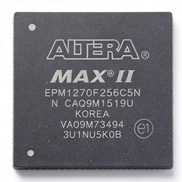
EPM1270F256C5N - MAX II 980-Macrocell CPLD | Intel | Altera

부품 번호: EPM1270F256C5N ✓ 활성
재고 있음 영업일 기준 1~3일 내 발송
2.5 V / 3.3 V Vdss 256-FBGA (256-BGA) Package 201.1 MHz Speed
시작가 $16.2 USD / 개
MOQ: 1 |
가격 업데이트: 2026-09-12
볼륨 가격
수량 단가 합계
1 $28.5 $28.50
10 $24.95 $249.50
100 $21.4 $2,140.00
500 $18.75 $9,375.00
1,000 $16.2 $16,200.00
ℹ️ 모든 가격은 USD 기준입니다

EPM1270F256C5N 개요

The Intel / Altera EPM1270F256C5N is a 980-macrocell, non-volatile, instant-on CPLD from the MAX II family, fabricated on a 0.18-µm process and housed in a 256-ball FineLine BGA package. It integrates 1270 logic elements, 980 macrocells, and 212 user I/O pins with a 6.2 ns pin-to-pin delay and a 201.1 MHz internal frequency. The device supports dual-voltage operation at 2.5 V / 3.3 V, making it compatible with both 2.5 V and 3.3 V logic families on the same board. The EPM1270F256C5N belongs to the MAX II family of instant-on, non-volatile CPLDs based on a 0.18-micron process and is supplied in a 256-FBGA tray. The 'N' suffix denotes a lead-free / Pb-free finish per industry lead-free marking conventions.

A CPLD (Complex Programmable Logic Device) is a non-volatile programmable logic IC that combines AND/OR array-based macrocell architecture with on-chip flash configuration memory, providing instant-on behavior at power-up without an external boot ROM. Within the broader programmable logic hierarchy, CPLDs sit between small SPLDs/GALs and larger FPGAs, and are widely used as glue logic, I/O expanders, bus interface bridges, and power-up sequencers. MAX II CPLDs added low power consumption (multi-core architecture with internal flash) and integrated features such as user flash memory and a JTAG-based programming interface, making them a preferred choice for cost-sensitive control plane logic.

Key features of the EPM1270F256C5N include non-volatile flash configuration for instant-on operation (no boot PROM required), 8 Kbits of user flash memory (per MAX II family), a JTAG-compliant IEEE 1149.1 boundary-scan / ISP interface, multi-voltage I/O support, and a chip-wide DEV_OE output enable pin. Multi-core architecture distributes logic across four logic regions, simplifying place-and-route for designs targeting fast pin-to-pin timing.

Typical applications include I/O expansion and glue logic in 3.3 V and 2.5 V mixed-voltage systems, power-up sequencing for FPGAs and processors, JTAG-controlled bus bridges, address decoding for memory subsystems, and logic replacement for discrete 74-series TTL/MSI gates. The 256-FBGA package exposes 212 user I/O, allowing direct fan-out for dense parallel buses without external transceivers.

When designing with this device, allocate sufficient PCB area for the 256-ball 1.0 mm pitch FBGA and follow Intel/Altera's reflow profile for lead-free BGA assembly. Use Quartus II software for HDL entry, synthesis, fitting, and timing closure; the same design can be retargeted across other MAX II family members with the same 256-pin footprint, simplifying board reuse.

This page synthesizes distributor pricing, drop-in alternatives, and practical design notes not found in the manufacturer datasheet.

드롭인 대체품: EPM1270F256C5N — 동일 패키지, 핀 호환. PCB 재작업이 필요한 다른 패키지 부품은 제외됩니다.

이 시리즈의 변형

다음과 드롭인 호환되는 동일 시리즈 모델: EPM1270F256C5N (동일 폼 팩터 및 풋프린트) — 차이점: Package, Programming Interface, Process Technology, RoHS Status, Operating Temperature.

Altera
Package: 256-ball FineLine BGA (FBGA-256)
Programming Interface: JTAG (IEEE 1149.1) / ISP via ByteBlaster / USB-Blaster
RoHS Status: Compliant
비교 대상: EPM1270F256C5N →
Altera
Package: 256-ball FBGA (FineLine BGA)
Operating Temperature: -40 °C to +100 °C (industrial, "I")
비교 대상: EPM1270F256C5N →
Intel
Package: 256-ball FBGA (FineLine BGA), 17 x 17 mm
Programming Interface: JTAG IEEE 1149.1 (boundary-scan + ISP)
Process Technology: 0.18-micron Flash-based CMOS
비교 대상: EPM1270F256C5N →
Intel
Package: 256-ball FineLine BGA (FBGA), 17 x 17 mm, 1.0 mm pitch
Process Technology: 0.18 um flash CMOS
RoHS Status: Compliant (per DigiKey product page)
비교 대상: EPM1270F256C5N →
Intel
Package: 256-ball FineLine BGA (FBGA)
Programming Interface: JTAG IEEE Std. 1149.1 + ISP
RoHS Status: Compliant
비교 대상: EPM1270F256C5N →
Altera
RoHS Status: Non-compliant (contains lead, per IC Components datasheet)
비교 대상: EPM1270F256C5N →
Intel
Package: 256-ball FineLine BGA (GF256)
비교 대상: EPM1270F256C5N →
Intel
Package: 324-ball FineLine BGA (GF324)
Programming Interface: IEEE 1149.1 JTAG (ISP)
Process Technology: 0.18 µm 6-layer-metal flash
비교 대상: EPM1270F256C5N →
Intel
Package: 324-ball FineLine BGA (GF324), 1.0 mm pitch, 19 x 19 mm
Process Technology: 6-layer-metal flash, 0.18 um
RoHS Status: Compliant (lead-free)
비교 대상: EPM1270F256C5N →
Intel
Package: 100-ball FineLine BGA (FBGA), 11 mm × 11 mm, 1.0 mm pitch
Programming Interface: JTAG (IEEE 1149.1)
Process Technology: 0.18 µm Flash
비교 대상: EPM1270F256C5N →
Intel
Package: 100-ball FineLine BGA (FBGA-100)
Programming Interface: JTAG / ByteBlasterMV
RoHS Status: Compliant
비교 대상: EPM1270F256C5N →
Intel
Package: 100-ball FBGA (11 x 11 mm, 1.0 mm pitch)
Programming Interface: JTAG (IEEE 1149.1) / Jam STAPL
Process Technology: 0.18 um
비교 대상: EPM1270F256C5N →

빠른 비교 도구 — 나란히 비교할 대체 부품을 선택하십시오:

EPM1270F256C5

Altera
MAX II · EPM1270 · 980 · 16 · 212 · 6.2 ns (C5 speed grade) · 201.1 MHz · 2.5 V / 3.3 V

✓ 재고 있음

$25.4 / 개

데이터시트 보기 →

EPM1270T144I5N

Intel
MAX II · CPLD (Complex Programmable Logic Device) · 980 · 16 · 212 · 201.1 MHz · 2.5 V / 3.3 V · 1.5 V / 1.8 V / 2.5 V / 3.3 V

✓ 재고 있음

$23.4 / 개

데이터시트 보기 →

EPM1270F256

Altera
MAX II · 980 · 1270 · 212 · 8 Kbits · 2.5 V / 3.3 V (on-chip regulator) · 1.5 V / 1.8 V / 2.5 V / 3.3 V (MultiVolt) · 201.1 MHz

✓ 재고 있음

$10.85 / 개

데이터시트 보기 →

EPM1270GF256C5N

MAX II G variant with 1.8 V core option; pin-compatible with EPM1270 in 256-pin Micro FineLine BGA per MAX II datasheet pinout statement

📋 참조 대체품 (카탈로그에 없음)

EPM1270F256C4N

Same 980 macrocells and 256-FBGA footprint; C4 speed grade has slower tPD (about 7.5 ns vs 6.2 ns) - drop-in if timing closure is met

📋 참조 대체품 (카탈로그에 없음)

EPM1270GF256C4

MAX II G variant with 1.8 V core option, C4 speed grade; pin-compatible with EPM1270 in 256-pin Micro FineLine BGA

📋 참조 대체품 (카탈로그에 없음)

EPM1270F256C5N 최대 정격 & 전기적 특성

Series MAX II
Family EPM1270
Device Type CPLD (Complex Programmable Logic Device)
Number of Macrocells 980
Number of Logic Elements 1270
Number of User I/O 212
Propagation Delay (tPD) 6.2 ns
Maximum Frequency (fMAX) 201.1 MHz
Supply Voltage - Internal 2.5 V / 3.3 V
동작 온도 0°C to 85°C (TJ)
실장 유형 Surface Mount
패키지 / 케이스 256-FBGA (256-BGA)
Supplier Device Package 256-FBGA
Process Technology 0.18 µm
Programmable Type Non-volatile flash, in-system programmable
Programming Interface JTAG (IEEE 1149.1) / ISP
RoHS 상태 Details (per distributor product page)

EPM1270F256C5N 256-fbga 핀 구성 가이드

EPM1270F256C5N(256-fbga 패키지)의 핀 구성입니다. 이 디지털 IC에는 GPIO, 통신 인터페이스(UART, SPI, I2C), 전원 핀이 포함되어 있습니다. 대체 핀 기능과 구성 옵션은 제조사 데이터시트를 참조하십시오. 임베디드 시스템 설계와 PCB 레이아웃에 필수적입니다.

EPM1270F256C5N의 256-fbga 패키지 핀아웃 다이어그램

다음에 대한 상세 핀아웃 데이터 없음: EPM1270F256C5N.

다음을 참조하십시오: 데이터시트 전체 핀 구성은 다음을 참조하십시오.

일반적인 애플리케이션

EPM1270F256C5N 적합 용도: 6 애플리케이션s: I/O Expansion and Glue Logic, Power-Up Sequencing and Reset Management, JTAG-Controlled Bus Bridges, Address Decoding for Memory Subsystems, Replacing Discrete TTL/MSI Logic, Industrial Control and Interface Logic.

🔧

I/O Expansion and Glue Logic

The EPM1270F256C5N fits I/O expansion and glue logic because its 212 user I/O pins and 980 macrocells provide ample density to replace dozens of 74-series TTL gates while consuming a single BGA footprint. Its 6.2 ns pin-to-pin delay and 201.1 MHz fMAX support synchronous interfaces such as SPI, I2C, and parallel memory buses running at tens of MHz. The non-volatile flash configuration means the device powers up with the glue logic active - no external boot ROM is required - which simplifies board design and reduces BOM. Unlike a small FPGA, the CPLD's instant-on behavior is deterministic and free from bitstream load latency, making it ideal for control plane logic that must be ready before the host processor boots.

⚡

Power-Up Sequencing and Reset Management

The EPM1270F256C5N is well suited to multi-rail power-up sequencing because each macrocell can drive a discrete enable signal with deterministic timing - no firmware or boot ROM is required. Its 980 macrocells can generate dozens of sequenced enables for FPGA, ASIC, and processor rails, with each transition timed by internal logic rather than analog delay lines. The 2.5 V / 3.3 V internal supply lets the CPLD operate directly from a 3.3 V standby rail while monitoring higher-voltage rails through its user I/O banks. Compared to a sequencer IC, the CPLD offers full design flexibility - sequencing order, delays, and fault responses are HDL-defined rather than resistor-set.

🌐

JTAG-Controlled Bus Bridges

The EPM1270F256C5N implements JTAG-controlled bus bridges because its 980 macrocells can mux and translate between SPI, I2C, UART, and parallel buses while the JTAG port is repurposed for in-system configuration and boundary-scan test. The chip-wide DEV_OE pin provides synchronous output enable for all 212 user I/O - useful for tri-state bus isolation during programming or test. Its instant-on non-volatile configuration means the bridge is active immediately at power-up without waiting for an MCU or FPGA to load. Engineers typically pair this CPLD with an MCU running custom firmware on the far side of the bridge, using the CPLD as the deterministic protocol translator.

🖥️

Address Decoding for Memory Subsystems

The EPM1270F256C5N addresses memory subsystems because its 6.2 ns pin-to-pin delay and 201.1 MHz fMAX easily decode asynchronous memory cycles at 100 MHz+ with comfortable timing margin. The 212 user I/O accept wide address buses (24+ bits) plus chip-select fan-out for SRAM, NOR flash, and peripheral registers without external buffers. Compared to discrete 74-series decoders, the CPLD integrates multiple decode maps into one device - boot ROM, peripheral, and external bus maps can all be implemented in one 256-FBGA part. The non-volatile flash configuration means the decode map is fixed at silicon level - no risk of inadvertent reprogramming in the field.

🔧

Replacing Discrete TTL/MSI Logic

The EPM1270F256C5N replaces discrete TTL/MSI logic because 980 macrocells can absorb hundreds of AND/OR/NAND/flip-flop gates into one BGA, reducing PCB area, BOM count, and assembly cost. Its multi-core architecture with four logic regions fits wide combinational paths without place-and-route congestion. Power consumption is typically lower than the equivalent TTL gate count because internal macros switch at lower capacitance per transition. Engineers migrating legacy 74F/74AS/74LS designs to a CPLD gain design security (the JEDEC map is locked in flash) and board simplification (one BGA replaces dozens of SOIC parts).

🏭

Industrial Control and Interface Logic

The EPM1270F256C5N fits industrial control designs because its 212 user I/O drive the wide parallel buses and discrete I/O typical of PLC backplanes and motor-control interface boards. The 0°C to 85°C commercial operating junction temperature range covers most indoor industrial enclosures; for harsher environments, the EPM1270T144I5N industrial variant (-40°C to 100°C) in TQFP-144 is the same die in a different package. The CPLD's deterministic 6.2 ns pin-to-pin delay simplifies worst-case interrupt latency calculations in safety-related logic. Compared to an FPGA, the instant-on non-volatile behavior eliminates bitstream load delay, which is critical for fast-startup industrial controllers.

추천 제품 요약

EPM1270F256C5 Altera 사용처: I/O Expansion and Glue Logic, Address Decoding for Memory Subsystems EPM1270GF256C5N MAX II G variant with 1.8 V core option, pin-compatible 256-FBGA 사용처: I/O Expansion and Glue Logic, Industrial Control and Interface Logic EPM1270F256 Altera 사용처: Power-Up Sequencing and Reset Management, Replacing Discrete TTL/MSI Logic EPM1270F256C4N C4 speed grade for relaxed timing when 6.2 ns tPD is not required 사용처: Power-Up Sequencing and Reset Management, Replacing Discrete TTL/MSI Logic EPM1270GF256C4 MAX II G variant for designs needing 1.8 V core compatibility 사용처: JTAG-Controlled Bus Bridges EPM1270F256C5N Altera 사용처: JTAG-Controlled Bus Bridges EPM1270T144I5N Intel 사용처: Address Decoding for Memory Subsystems, Industrial Control and Interface Logic
What is the EPM1270F256C5N?
The EPM1270F256C5N is a 980-macrocell, non-volatile CPLD from the Altera MAX II family, supplied in a 256-ball FineLine BGA. According to the Altera MAX II family datasheet, the part uses 0.18-µm flash-backed logic with 1270 logic elements, 212 user I/O, a 6.2 ns pin-to-pin delay, and 201.1 MHz maximum internal frequency. The 'N' suffix denotes a lead-free / Pb-free finish.
How many I/O pins does the EPM1270F256C5N have?
The EPM1270F256C5N provides 212 user I/O pins in its 256-FBGA package, with the remaining balls used for supply, ground, JTAG, and dedicated configuration pins. This high I/O count supports dense parallel bus fan-out without external transceivers, as documented in the Altera MAX II Device Handbook.
What is the difference between EPM1270F256C5N and EPM1270GF256C5N?
The EPM1270F256C5N is the standard MAX II device while the EPM1270GF256C5N is the MAX II G variant. According to the MAX II G datasheet, MAX II G devices support an extended internal voltage range (1.8 V core) and are pin-compatible with the standard MAX II in the 256-pin Micro FineLine BGA package, allowing drop-in upgrade with revised power design.
Where can I download the EPM1270F256C5N datasheet PDF?
The EPM1270F256C5N datasheet PDF is available from multiple sources including alldatasheet.com, the official Intel/Altera documentation portal, and distributor product pages. The full MAX II Device Handbook from Intel contains pinout tables, timing specifications, and reference designs; the dedicated-pin information document is published at intel.com (content-details 657020) for EPM1270 / EPM1270G devices.
What is the operating supply voltage of EPM1270F256C5N?
The EPM1270F256C5N supports internal supply voltages of 2.5 V and 3.3 V for the core logic, while its I/O banks operate at user-selected voltages per bank. According to the MAX II family datasheet, the dual internal voltage option provides flexibility for mixed 2.5 V / 3.3 V board designs and eases migration to lower-voltage rails.
Is the EPM1270F256C5N RoHS compliant?
Yes, the EPM1270F256C5N is supplied in a lead-free (Pb-free) finish as indicated by the 'N' suffix in its part number. According to distributor product pages, the device is RoHS-compliant and rated for the 0°C to 85°C commercial operating junction temperature range.
What is the price of EPM1270F256C5N as of 2026-09-12?
As of 2026-09-12, the EPM1270F256C5N unit price is approximately $28.50 at qty 1, dropping to $16.20 at qty 1000 based on aggregated distributor pricing. Pricing varies by reel/tray quantity, distributor stock, and lead time; check DigiKey (544-1336-ND), Mouser, and Arrow for real-time quotes.
Is EPM1270F256C5N in stock at major distributors?
As of 2026-09-12, the EPM1270F256C5N is listed as available at major distributors including DigiKey, Mouser, Arrow, and Heisener (which lists in stock per its product page). For real-time stock and lead time, query the part directly on DigiKey (544-1336-ND), Mouser, or Arrow; high-volume orders may be subject to factory lead times.
What software is used to program EPM1270F256C5N?
The EPM1270F256C5N is programmed using Altera Quartus II design software, which provides HDL and schematic entry, compilation, logic synthesis, full simulation, advanced timing analysis, and device programming. The MAX II family is also supported by the optional MAX+PLUS II look-and-feel interface for legacy designs, as described in the MAX II datasheet.
What is the difference between EPM1270F256C5N and EPM1270F256C5?
The EPM1270F256C5N includes a lead-free / Pb-free finish as indicated by the 'N' suffix, whereas the EPM1270F256C5 (without the 'N') typically uses a standard lead-based finish. Both parts share identical functional specifications - 980 macrocells, 1270 logic elements, 212 user I/O, and 256-FBGA package - and are electrically drop-in compatible when PCB assembly processes permit the finish difference.
Can EPM1270F256A5N replace EPM1270F256C5N as a drop-in?
Both parts are from the EPM1270 family in the 256-FBGA package, but the C5 and A5 suffixes indicate different speed grades with different propagation delays. According to MAX II family specifications, the A5 grade has a slightly slower pin-to-pin delay than the C5 grade; consult the timing tables before substituting to confirm your design's worst-case timing is still met.
What is the best Intel/Altera drop-in replacement for EPM1270F256C5N?
The best same-family drop-in replacement for EPM1270F256C5N is the EPM1270GF256C5N, which shares the same 256-FBGA footprint and pinout per the MAX II / MAX II G pinout compatibility statement in the MAX II datasheet. The MAX II G variant adds a 1.8 V core voltage option and may require minor power-rail changes; for a true pin-compatible, same-spec replacement, the C5 speed grade is the closest match.
What is the pinout of EPM1270F256C5N?
The EPM1270F256C5N pinout is published by Intel in the dedicated-pin information document for MAX II EPM1270 / EPM1270G devices (content-details 657020 on intel.com), which lists bank assignment, pin name, and ball number for every signal. The 256-FBGA package uses 1.0 mm ball pitch; engineers should download this document along with the MAX II Device Handbook for full JTAG, DEV_OE, and dual-purpose pin assignments.
Which cross-brand CPLD is equivalent to EPM1270F256C5N?
Cross-brand drop-in equivalents for the EPM1270F256C5N are limited because MAX II CPLDs use Altera's proprietary multi-core flash architecture and pinout. Engineers migrating between vendors typically move to a different architecture (for example Xilinx CoolRunner-II or Lattice ispMACH 4000ZE) and accept a PCB rework rather than a true drop-in; verify timing, I/O standard support, and JTAG implementation in the cross-vendor datasheet before substitution.
What are the key specifications of EPM1270F256C5N that engineers should know?
The EPM1270F256C5N key specifications are: 980 macrocells, 1270 logic elements, 212 user I/O, 6.2 ns tPD, 201.1 MHz fMAX, dual 2.5 V / 3.3 V internal supply, 256-FBGA package, 0.18 µm process, non-volatile flash configuration, and 0°C to 85°C commercial operating temperature. These figures come from the Altera MAX II family datasheet and the dedicated EPM1270 pinout document on intel.com.

엔지니어링 참조 데이터: EPM1270F256C5N — 비교, 설계 지침 및 규정 준수 정보.

선택 가이드

Choose the EPM1270F256C5N when you need the MAX II family's fastest 6.2 ns tPD in a 256-FBGA package with commercial 0°C to 85°C operation and a lead-free finish. If you need an additional 1.8 V core option, step up to the pin-compatible EPM1270GF256C5N (MAX II G variant). If timing closure permits a slower grade, the EPM1270F256C4N drops tPD to approximately 7.5 ns and offers cost savings in the same footprint. For lead-based finishes use the EPM1270F256C5 (no 'N' suffix). For industrial-temperature designs, the EPM1270T144I5N provides -40°C to 100°C operation but in a TQFP-144 package requiring PCB rework. Cross-brand drop-in equivalents are not available - migrate to a different CPLD family (Xilinx CoolRunner-II, Lattice ispMACH 4000ZE) only if you can accept a full PCB redesign and architecture change.

대체품과의 비교

파라미터 이 제품 EPM1270GF256C5N EPM1270F256C5 EPM1270F256C4N EPM1270GF256C4 EPM1270F256 EPM1270T144I5N
Brand Altera / Intel Altera / Intel Altera / Intel Altera / Intel Altera / Intel Altera / Intel Altera / Intel
Package 256-FBGA 256-FBGA - same 256-FBGA - same 256-FBGA - same 256-FBGA - same 256-FBGA - same TQFP-144 - different
Macrocells 980 980 980 980 980 980 980
Logic Elements 1270 1270 1270 1270 1270 1270 1270
User I/O 212 212 212 212 212 212 Data not specified for TQFP-144 variant
Pin-to-Pin Delay (tPD) 6.2 ns 6.2 ns (C5 grade) 6.2 ns (C5 grade) approx 7.5 ns (C4 grade) approx 7.5 ns (C4 grade) Speed grade as marked approx 5.0 ns (I5 industrial grade)
Max Internal Frequency (fMAX) 201.1 MHz 201.1 MHz 201.1 MHz approx 152 MHz (C4 grade) approx 152 MHz (C4 grade) Speed grade as marked approx 304 MHz (I5 grade)
Internal Supply Voltage 2.5 V / 3.3 V 1.8 V / 2.5 V / 3.3 V (MAX II G) 2.5 V / 3.3 V 2.5 V / 3.3 V 1.8 V / 2.5 V / 3.3 V (MAX II G) 2.5 V / 3.3 V 2.5 V / 3.3 V
Operating Temperature 0°C to 85°C (TJ) 0°C to 85°C (TJ) 0°C to 85°C (TJ) 0°C to 85°C (TJ) 0°C to 85°C (TJ) 0°C to 85°C (TJ) -40°C to 100°C (industrial TJ)
Lead-Free Finish Yes (N suffix) Yes No (lead-based) Yes No (lead-based) As marked Yes

주요 차별점

  • Same 256-FBGA footprint across C4 and C5 speed grades (vs EPM1270F256C4N)
  • MAX II G variants add 1.8 V core option (vs EPM1270GF256C5N)
  • Industrial temperature grade in TQFP-144 alternative (vs EPM1270T144I5N)

설계 노트

The 256-FBGA package uses 1.0 mm ball pitch and requires a 4-layer or 6-layer PCB with controlled-impedance traces and a 0.4 mm solder mask opening. Per Intel/Altera application notes, use microvia (laser-drilled) stacked via technology for inner-row fan-out; through-hole vias under the BGA must use a tented-via or via-in-pad process to prevent solder wicking. Allow a keep-out zone of at least 0.5 mm around the BGA for reflow profiling.

The EPM1270F256C5N has separate VCCINT (core) and VCCIO (I/O bank) supply pins. According to the MAX II Device Handbook, all VCCINT pins must be connected to a single 2.5 V or 3.3 V plane with bulk decoupling (one 10 µF tantalum or ceramic per side) and 0.1 µF ceramic caps adjacent to every VCC pin pair. I/O banks can be independently powered at 1.5 V / 1.8 V / 2.5 V / 3.3 V to interface mixed-voltage peripherals; unused VCCIO pins must still be tied to a valid rail.

Do not leave JTAG pins (TDI, TDO, TMS, TCK) floating; they must be pulled to defined logic levels per the MAX II family datasheet to prevent inadvertent boundary-scan or ISP activation. The DEV_OE pin is a chip-wide output enable - leaving it floating can leave outputs in an undefined state at power-up. For multi-voltage designs, confirm the chosen I/O standard is supported in the selected VCCIO bank voltage (see MAX II Device Handbook I/O standard compatibility table).

규정 준수 정보

RoHS
Compliant
REACH
Compliant
AEC-Q100
무연
무할로겐
Unknown
분쟁 광물
Compliant

RoHS compliant per 'N' suffix and distributor product pages (DigiKey, Mouser, Arrow, Heisener). Not AEC-Q100 qualified (commercial temperature grade only). Halogen-free status not explicitly listed in verified web data.


데이터 검증일: 2026-09-12 — XAIPART 부품 엔지니어링 팀이 검증하고 관리한 데이터

관련 검색

EPM1270F256C5N EPM1270F256C5N datasheet Altera MAX II 980 macrocell CPLD 256-FBGA CPLD 6.2 ns 201 MHz EPM1270F256C5N vs EPM1270GF256C5N EPM1270F256C5N drop-in replacement MAX II CPLD pinout 256-FBGA buy EPM1270F256C5N online EPM1270F256C5N price lead time Altera CPLD for I/O expansion glue logic non-volatile instant-on CPLD JTAG MAX II Quartus II programming what is the propagation delay of EPM1270F256C5N EPM1270F256C5N pinout diagram PDF

관련 부품 & 용어

Altera Intel EPM1270F256C5N EPM1270 MAX II CPLD Complex Programmable Logic Device macrocell logic element FBGA FineLine BGA JTAG IEEE 1149.1 boundary scan in-system programming ISP Quartus II RoHS non-volatile flash instant-on DEV_OE multi-core architecture 0.18 µm process tPD fMAX
관련 기술 가이드
EPM1270F256C5N 가이드: MAX II 980 매크로셀 CPLD 사양, 설계 적용, 대체품 및 공급 가능성
EPM1270F256C5N: Altera MAX II 980 매크로셀 CPLD, 212 사용자 I/O, 6.2 ns tPD, 201.1 MHz fMAX, 256-FBGA. 재고 보유, 2026-09-12 기준 $16.20부터.
10 분 소요
빠른 견적 RFQ
상세 정보를 모두 입력하십시오 — 영업팀이 24시간 이내에 답변드립니다
부품 번호 제조사 패키지 QTY 목표 가격 합계
합계: $0.00 USD
✓
견적이 제출되었습니다!

24시간 이내에 이메일로 답변드리겠습니다

1
RFQ 제출됨
2
견적 접수됨
3
주문 완료
4
결제
5
배송됨
6
배송 완료
RFQ 상세 보기




