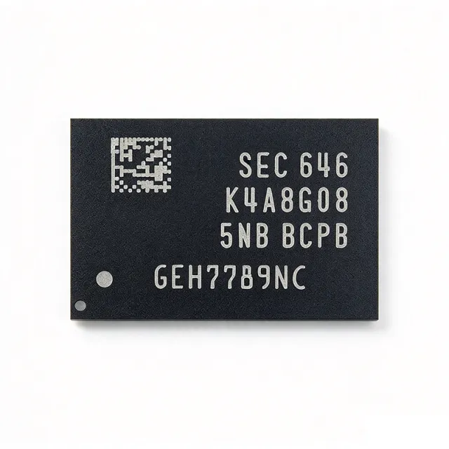
K4A8G085WB-BCPB - 8Gb DDR4 SDRAM 1Gx8 1.2V | Samsung
부품 번호: K4A8G085WB-BCPB ✓ 활성| 수량 | 단가 | 합계 |
|---|---|---|
| 1 | $7.0313 | $7.03 |
| 10 | $5.0781 | $50.78 |
| 100 | $4.4922 | $449.22 |
| 500 | $4.2969 | $2,148.45 |
| 1,000 | $4.1016 | $4,101.60 |
K4A8G085WB-BCPB 개요
DDR4 SDRAM is the fourth generation of double-data-rate synchronous dynamic random-access memory. As a volatile DRAM technology, it sits at the top of the memory hierarchy below CPU caches, providing the working memory for processors in servers, PCs, and embedded systems. Compared with DDR3, DDR4 lowers operating voltage from 1.5V to 1.2V, increases bank counts, and introduces bank-group architecture for higher effective data rates and improved power efficiency.
Key features of this device include the 8Gbit density in a x8 organization, 1.2V core supply, a maximum clock frequency of up to 1066 MHz (DDR4-2133 data-rate class per distributor documentation), and the industry-standard 78-ball FBGA footprint that enables dense module and solder-down designs. The B-die family is well known in the enthusiast and embedded communities for its timing headroom.
Architecturally, the K4A8G085WB-BCPB implements DDR4 bank groups, on-die termination (ODT), DLL-enabled operation, and programmable CAS latency per the JEDEC DDR4 SDRAM specification. Samsung notes that the datasheet is an abstract of the full DDR4 specification and that timing figures apply to DLL-enabled mode; common operational features are covered in the companion DDR4 SDRAM Device Operation & Timing Diagram document.
Typical applications include desktop and notebook DIMM modules, server RDIMM/LRDIMM memory subsystems, embedded single-board computers, networking equipment, and industrial controllers requiring high-bandwidth volatile memory. The x8 organization suits controllers with 64-bit or 72-bit (ECC) memory buses needing 8 or 9 devices per rank.
Design consideration: DDR4 signal integrity demands length-matched routing, controlled impedance, and correct VTT/VPP termination; verify speed-grade bin (BCPB) timing parameters against your memory controller configuration before layout.
This page synthesizes distributor pricing, drop-in alternatives, and practical design notes not found in the manufacturer datasheet, with pricing as of 2026-09-04.
드롭인 대체품: K4A8G085WB-BCPB — 동일 패키지, 핀 호환. PCB 재작업이 필요한 다른 패키지 부품은 제외됩니다.
빠른 비교 도구 — 나란히 비교할 대체 부품을 선택하십시오:
K4A8G085WB-BCRC
✓ 재고 있음
$6.8 / 개
데이터시트 보기 →K4A8G085WB-BITD
✓ 재고 있음
$3.8 / 개
데이터시트 보기 →K4A8G085WC-BIWE
✓ 재고 있음
$6.29 / 개
데이터시트 보기 →K4A8G085WG-BCWE
📋 참조 대체품 (카탈로그에 없음)
K4A8G085WG-BIWE
📋 참조 대체품 (카탈로그에 없음)
K4A8G085WB-BCPB 최대 정격 & 전기적 특성
| 메모리 유형 | DDR4 SDRAM (volatile DRAM) |
| 메모리 크기 | 8 Gb |
| Memory Organization | 1G x 8 |
| 공급 전압 | 1.2 V |
| Max Clock Frequency | 1066 MHz |
| Max Access Time | 0.18 ns |
| Max Standby Current | 0.016 mA |
| Refresh Cycles | 8192 |
| Technology | CMOS, 8Gb B-die |
| 패키지 | 78-ball FBGA (BGA78 / TFBGA), rectangular, 11 mm length |
| Number of Terminals | 78 |
| 실장 유형 | Surface Mount |
| 동작 온도 | 0C to +85C |
| 인터페이스 | DDR4 SDRAM parallel interface |
| Operating Temperature Grade | Commercial (0C to 85C) |
K4A8G085WB-BCPB 78-ball fbga (bga78 / tfbga), rectangular, 11 mm length 핀 구성 가이드
K4A8G085WB-BCPB(78-ball fbga (bga78 / tfbga), rectangular, 11 mm length 패키지)의 핀 구성입니다. 이 디지털 IC에는 GPIO, 통신 인터페이스(UART, SPI, I2C), 전원 핀이 포함되어 있습니다. 대체 핀 기능과 구성 옵션은 제조사 데이터시트를 참조하십시오. 임베디드 시스템 설계와 PCB 레이아웃에 필수적입니다.

다음에 대한 상세 핀아웃 데이터 없음: K4A8G085WB-BCPB.
다음을 참조하십시오: 데이터시트 전체 핀 구성은 다음을 참조하십시오.
일반적인 애플리케이션
K4A8G085WB-BCPB 적합 용도: 6 애플리케이션s: Desktop and Notebook DIMM Modules, Server Memory Subsystems, Embedded Single-Board Computers, Networking and Communication Equipment, Industrial Automation Controllers, Test and Measurement Instruments.
Desktop and Notebook DIMM Modules
The K4A8G085WB-BCPB is a primary DRAM component for UDIMM and SODIMM memory modules in desktop and notebook PCs. Its 8Gb density in x8 organization allows 16 modules per 16GB dual-rank DIMM, and the DDR4-2133 class speed matches mainstream host memory controllers. With a 1.2V core supply versus DDR3's 1.5V, system memory power drops roughly 20% at the module level, directly improving laptop battery runtime. Mounted on the module PCB with fly-by command/address routing and per-rank on-die termination, the FBGA-78 packages support high signal integrity at 1066 MHz clock rates. Designers should follow JEDEC module layout guidance for trace length matching and VTT decoupling.
추천
Server Memory Subsystems
In server platforms, the K4A8G085WB-BCPB populates RDIMM and LRDIMM ranks where 8Gb density minimizes device count per gigabyte. The x8 organization aligns with 72-bit ECC buses (64 data + 8 check bits), requiring exactly nine x8 devices per rank. At 1.2V and DDR4-2133 class bandwidth, the part balances throughput and thermal load in dense 2U storage servers. Samsung's B-die DDR4 family is widely used in hyperscale deployments where refresh (8192 cycles per 64 ms) and RAS features maintain data integrity. For higher-bandwidth server tiers, the DDR4-3200 class K4A8G085WG-BCWE offers the same footprint with faster bins, allowing a single PCB layout to serve multiple performance SKUs.
추천
Embedded Single-Board Computers
Embedded SBCs and COM express modules solder the K4A8G085WB-BCPB directly to the carrier PCB, eliminating SO-DIMM connectors to save space, height, and cost. The 78-ball FBGA's 11 mm rectangular body fits low-profile fanless enclosures, and 8Gb provides ample working memory for Linux-based industrial gateways and HMI platforms. The commercial 0C to +85C range suits indoor industrial environments; deployments beyond that should use the industrial-grade K4A8G085WB-BITD. Designers must implement DDR4 fly-by routing with length matching within ±25 mils on address/command groups, reference-plane-continuous stackups, and VTT termination islands near the DRAM ball field, per Samsung's DDR4 PCB design guidelines.
추천
Networking and Communication Equipment
Routers, switches, and 5G small-cell equipment use K4A8G085WB-BCPB as packet-buffer and control-plane memory. DDR4-2133 class bandwidth sustains line-rate buffering in access equipment, while the 1Gx8 organization lets designers scale bus width in eight-bit increments to match network processor memory controllers. The 1.2V core supply reduces total system power, which is critical in fanless telecom hardware with strict thermal budgets. Burst-oriented DDR4 operation with bank-group interleaving keeps random-access latency low for irregular packet traffic patterns. For aggregation platforms needing DDR4-3200 throughput, the footprint-compatible K4A8G085WC-BIWE enables bandwidth upgrades without PCB respin.
추천
Industrial Automation Controllers
PLC CPUs, motion controllers, and machine-vision edge computers employ the K4A8G085WB-BCPB as main memory for deterministic control code and image frame buffers. The 8Gb per device permits 2GB arrays with only sixteen packages, simplifying BOM and reflow processes. At 1.2V and a maximum standby current of just 0.016 mA, the DRAM contributes negligibly to idle power in always-on factory equipment. Machine-vision pipelines particularly benefit from DDR4 burst bandwidth when streaming multi-megapixel sensor frames into frame buffers. Control cabinets typically stay within the 0C to +85C commercial envelope; for outdoor or cold-storage deployments, substitute the industrial-grade K4A8G085WB-BITD, which shares the identical FBGA-78 footprint.
추천
Test and Measurement Instruments
Oscilloscopes, logic analyzers, and protocol analyzers use the K4A8G085WB-BCPB in deep-capture memory banks where 8Gb density extends record length without expanding board area. A bank of sixteen devices yields 16 GB of capture memory, essential for long-timebase signal debugging. The DDR4-2133 class interface sustains the sustained streaming rates demanded when transferring acquisition data to the analysis processor. The 0.18 ns access time and DLL-enabled operation ensure deterministic timing referenced to the acquisition clock domain. Benchtop instruments operate in climate-controlled environments well inside the 0C to +85C rating, making the commercial-grade BCPB bin an appropriate, cost-effective choice for instrumentation memory subsystems.
추천
추천 제품 요약
엔지니어링 참조 데이터: K4A8G085WB-BCPB — 비교, 설계 지침 및 규정 준수 정보.
선택 가이드
대체품과의 비교
| 파라미터 | 이 제품 | K4A8G085WB-BCRC | K4A8G085WB-BITD | K4A8G085WC-BIWE | K4A8G085WG-BCWE |
|---|---|---|---|---|---|
| Package | FBGA-78 (BGA78) | FBGA-78 - same | FBGA-78 - same | FBGA-78 - same | FBGA-78 - same |
| Brand | Samsung Electronics | Samsung Electronics | Samsung Electronics | Samsung Electronics | Samsung Electronics |
| Memory Size | 8 Gb | 8 Gb | 8 Gb | 8 Gb | 8 Gb |
| Organization | 1G x 8 | 1G x 8 | 1G x 8 | 1G x 8 | 1G x 8 |
| Supply Voltage | 1.2 V | 1.2 V | 1.2 V | 1.2 V | 1.2 V |
| Speed Class | DDR4-2133 (1066 MHz clock) | DDR4-2666 class | DDR4-2133 class | DDR4-3200 class | DDR4-3200 Mbps |
| Refresh Cycles | 8192 | 8192 | 8192 | 8192 | 8192 |
주요 차별점
- Cost-optimized mainstream speed bin (vs K4A8G085WC-BIWE)
- Proven B-die silicon family (vs K4A8G085WG-BIWE)
- Footprint compatibility across speed and temperature grades (vs K4A8G085WB-BITD)
설계 노트
DDR4 solder-down layout demands strict length matching and reference-plane discipline. Route address/command/control in fly-by topology with intra-group skew under +/-25 mils, match DQ byte lanes to their DQS pairs within +/-5 mils, and keep all DDR4 traces on a continuous ground reference plane - never cross plane splits. Samsung's DDR4 design guides and JEDEC module layouts are the authoritative references; follow the 78-ball FBGA fanout escape pattern recommended for 0.8 mm ball pitch to allow via access under the package.
Plan three rails for DDR4: 1.2V VDD core, 2.5V VPP, and VTT termination at VDD/2 (0.6V). VTT must source and sink termination current during read/write bursts, so use a dedicated VTT LDO or switching terminator with bulk capacitance at the DRAM ball field. The BCPB's low standby current (0.016 mA max per distributor data) helps idle power, but termination current dominates active draw - size the VTT regulator for worst-case bus switching on all DQ/DQS/ADDR lines simultaneously.
Do not mix speed bins without re-verifying the memory controller initialization table: a BCRC or WC part dropped into a BCPB-timed socket must be programmed with its own CAS latency and speed bin, or training may fail at boot. Also confirm temperature grade: the BCPB is commercial (0C to +85C) and is not qualified for industrial extremes - select K4A8G085WB-BITD instead. Finally, note that Samsung's datasheet is an abstract; consult the companion DDR4 Device Operation & Timing Diagram for refresh, self-refresh, and mode-register details.
규정 준수 정보
Compliance data not present in the provided web data. Samsung DRAM products are typically RoHS compliant, but confirm on the official Samsung product page before procurement.


