STMicroelectronics

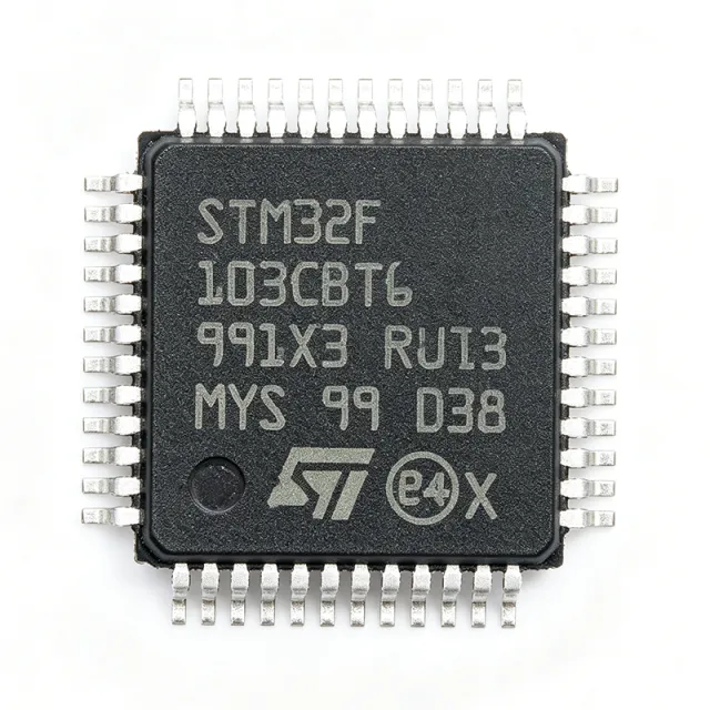
STM32F103CBT6 - 72MHz Cortex-M3 128KB Flash MCU | STMicroelectronics

부품 번호: STM32F103CBT6 ✓ 활성
재고 있음 영업일 기준 1~3일 내 발송
2.0 V to 3.6 V Vdss LQFP-48 (7x7 mm) Package 72 MHz Speed 128 KB Memory
시작가 $3.2 USD / 개
MOQ: 1 |
가격 업데이트: 2026-10-10
볼륨 가격
수량 단가 합계
1 $5.62 $5.62
10 $5.05 $50.50
100 $4.4 $440.00
500 $3.78 $1,890.00
1,000 $3.2 $3,200.00
ℹ️ 모든 가격은 USD 기준입니다

STM32F103CBT6 개요

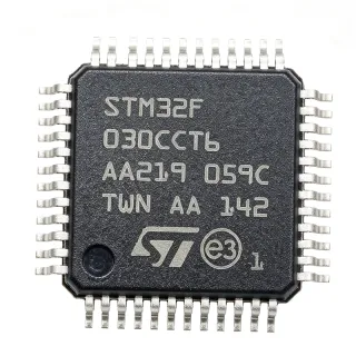
The STMicroelectronics STM32F103CBT6 is a 32-bit ARM Cortex-M3 mainstream microcontroller running at up to 72 MHz with 128 KB of Flash and 20 KB of SRAM, packaged in a 48-pin LQFP (7x7 mm) device.

What is a microcontroller? An MCU integrates a processor core, on-chip non-volatile memory (Flash), volatile working memory (SRAM), and a set of programmable peripherals onto a single silicon die. Within the embedded-computing hierarchy it sits above a bare microprocessor and below a full system-on-chip, and within ST's own portfolio the STM32F1 mainstream series places the STM32F103CBT6 between the ultra-low-power STM32L family and the higher-performance Cortex-M4 STM32F4 family. The part belongs to the medium-density STM32F103xx performance line, which targets cost-sensitive industrial and consumer control.

Key features include a 72 MHz Cortex-M3 core with single-cycle hardware multiply and divide, a 2.0 V to 3.6 V supply range, an embedded nested vectored interrupt controller with 43 maskable channels, and up to 37 GPIO pins tolerant to 5 V. On-board communication is broad for the class: three USARTs, two I2C buses, two SPI interfaces, one full-speed USB 2.0 device port, and one CAN 2.0B active controller. Two 12-bit ADCs (1 us conversion), one 12-bit DAC, three general-purpose 16-bit timers, one PWM timer, and one basic timer give ample motor-control flexibility.

Technically, the clock tree uses an internal 8 MHz RC oscillator plus a 4-16 MHz external crystal and a dedicated 32 kHz RTC oscillator; PLL multiplication reaches 72 MHz. Programming is via SWD or JTAG, with a built-in bootloader selectable via BOOT0/BOOT1. The 7x7 mm LQFP-48 package gives a low-cost, easy-to-assemble footprint suitable for both hand-soldered prototypes and high-volume SMT lines.

Typical applications include industrial control nodes, motor drives, USB-to-CAN fieldbus bridges, medical instruments, smart-home hubs, and IoT gateways, where the combination of USB, CAN, and multiple UARTs positions the part as a communication-rich embedded hub. For design, decouple every VDD pin with 100 nF ceramics plus a single 4.7 uF bulk, place the HSE crystal traces short and guarded, and tie BOOT0 to GND for normal Flash boot or to VDD for system-memory bootloader. This page synthesises distributor pricing, drop-in alternatives (GD32F103CBT6, APM32F103CBT6, AT32F403ACBT7), and practical design notes not found in the ST datasheet.

드롭인 대체품: STM32F103CBT6 — 동일 패키지, 핀 호환. PCB 재작업이 필요한 다른 패키지 부품은 제외됩니다.

이 시리즈의 변형

다음과 드롭인 호환되는 동일 시리즈 모델: STM32F103CBT6 (동일 폼 팩터 및 풋프린트) — 차이점: Package, ADC, Timers, Communication Interfaces, Flash Memory.

STMicroelectronics
Package: LQFP-48
Communication Interfaces: USART (2), SPI (2), I2C (2), USB 2.0 FS, CAN 2.0B
Flash Memory: 64 KB
비교 대상: STM32F103CBT6 →
STMicroelectronics
Package: 48-LQFP (7x7 mm)
ADC: 2 x 12-bit, 1 MSPS, up to 10 channels
Timers: 7 x 16-bit (incl. PWM)
비교 대상: STM32F103CBT6 →
STMicroelectronics
Package: 48-UFQFPN, 7 mm x 7 mm
ADC: 2 ADCs
Timers: 7 timers
비교 대상: STM32F103CBT6 →
STMicroelectronics
Package: LQFP-64 (10x10 mm)
ADC: 2 x 12-bit, 1 us conversion, up to 16 channels
Timers: 7 x 16-bit (including PWM)
비교 대상: STM32F103CBT6 →
STMicroelectronics
Package: 64-LQFP 10 x 10 mm
ADC: Two ADCs
Timers: Seven 16-bit timers
비교 대상: STM32F103CBT6 →
STMicroelectronics
Package: LQFP-100 (14 x 14 mm)
ADC: 2 x 12-bit, up to 16 channels
Timers: 3 x 16-bit GP timers, 1 x advanced PWM timer
비교 대상: STM32F103CBT6 →

빠른 비교 도구 — 나란히 비교할 대체 부품을 선택하십시오:

STM32F103C8T6

✅ 드롭인
STMicroelectronics
📦 LQFP-48 (7x7 mm)
ARM Cortex-M3 · 72 MHz · 64 KB · 20 KB · 2.0 V to 3.6 V · -40C to +85C · LQFP-48 · Surface Mount

✓ 재고 있음

$1.02 / 개

데이터시트 보기 →

STM32F103RBT6

✅ 드롭인
STMicroelectronics
📦 LQFP-48 (7x7 mm)
ARM Cortex-M3 32-bit RISC · 72 MHz · 1.25 DMIPS/MHz · 128 KB · 20 KB · 2.0 V to 3.6 V · -40 C to +85 C (industrial grade) · LQFP-64 (10x10 mm)

✓ 재고 있음

$3.18 / 개

데이터시트 보기 →

STM32F103VBT6

✅ 드롭인
STMicroelectronics
📦 LQFP-48 (7x7 mm)
ARM Cortex-M3 32-bit · 72 MHz · 90 DMIPS (1.25 DMIPS/MHz) · 128 KB · 20 KB · 2.0 V to 3.6 V · 2 x 12-bit, up to 16 channels · 3 x 16-bit GP timers, 1 x advanced PWM timer

✓ 재고 있음

$3.33 / 개

데이터시트 보기 →

GD32F103CBT6

✅ 드롭인
📦 LQFP-48 (7x7 mm)
Up to 108 MHz core clock (+50% vs ST 72 MHz), 1.2 V internal LDO; identical register map for most peripherals

📋 참조 대체품 (카탈로그에 없음)

APM32F103CBT6

✅ 드롭인
📦 LQFP-48 (7x7 mm)
Geehy/Apmix part, up to 96 MHz core, register-compatible with STM32F103 series per datasheet

📋 참조 대체품 (카탈로그에 없음)

CKS32F103CBT6

✅ 드롭인
📦 LQFP-48 (7x7 mm)
CKS (CKSEMI) clone, 72 MHz parity mode, CMSIS startup compatible

📋 참조 대체품 (카탈로그에 없음)

AT32F403ACBT7

✅ 드롭인
📦 LQFP-48 (7x7 mm)
Artery Cortex-M4 up to 240 MHz, ~2x DSP performance, pin-compatible LQFP-48 (requires recompilation)

📋 참조 대체품 (카탈로그에 없음)

STM32F103CBT6 최대 정격 & 전기적 특성

Core ARM Cortex-M3 32-bit RISC
최대 클록 주파수 72 MHz
Flash Memory 128 KB
SRAM 20 KB
공급 전압 2.0 V to 3.6 V
GPIO Count 37 (5 V tolerant)
ADC 2x 12-bit, up to 10 channels
DAC 1x 12-bit
Timers 3x 16-bit GP + 1x PWM + 1x basic
USART 3
I2C 2
SPI 2
USB USB 2.0 Full-Speed Device
CAN 1x CAN 2.0B Active
패키지 LQFP-48 (7x7 mm)
동작 온도 -40 C to +85 C
실장 유형 Surface Mount
RoHS 상태 Compliant

STM32F103CBT6 핀 구성

LQFP-48 Package Pinout Diagram LQFP-48 7x7mm, P0.5mm, JEDEC MS-026. 1 12 LQFP-48
핀 1 VBAT — RTC backup supply
핀 2 PC13 — GPIO/Tamper-RTC (5V tolerant)
핀 3 PC14 — GPIO/OSC32_IN (5V tolerant)
핀 4 PC15 — GPIO/OSC32_OUT (5V tolerant)
핀 5 OSC_IN — HSE crystal input
핀 6 OSC_OUT — HSE crystal output
핀 7 NRST — Reset (active low)
핀 8 VSSA — Analog ground
핀 9 VDDA — Analog supply (2.0-3.6 V)
핀 10 PA0 — GPIO/ADC0/WKUP
핀 11 PA1 — GPIO/ADC1
핀 12 PA2 — GPIO/USART2_TX/ADC2
핀 13 PA3 — GPIO/USART2_RX/ADC3
핀 14 PA4 — GPIO/SPI1_NSS/ADC4
핀 15 PA5 — GPIO/SPI1_SCK/ADC5
핀 16 PA6 — GPIO/SPI1_MISO/ADC6
핀 17 PA7 — GPIO/SPI1_MOSI/ADC7
핀 18 PB0 — GPIO/ADC8
핀 19 PB1 — GPIO/ADC9
핀 20 PB2 — GPIO/BOOT1
핀 21 PB10 — GPIO/I2C2_SCL/USART3_TX
핀 22 PB11 — GPIO/I2C2_SDA/USART3_RX
핀 23 VSS_1 — Digital ground
핀 24 VDD_1 — Digital supply (2.0-3.6 V)
핀 25 PB12 — GPIO/SPI2_NSS
핀 26 PB13 — GPIO/SPI2_SCK
핀 27 PB14 — GPIO/SPI2_MISO
핀 28 PB15 — GPIO/SPI2_MOSI
핀 29 PA8 — GPIO/TIM1_CH1
핀 30 PA9 — GPIO/USART1_TX
핀 31 PA10 — GPIO/USART1_RX
핀 32 PA11 — GPIO/USBDM/CAN_RX
핀 33 PA12 — GPIO/USBDP/CAN_TX
핀 34 PA13 — GPIO/SWDIO
핀 35 VSS_2 — Digital ground
핀 36 VDD_2 — Digital supply (2.0-3.6 V)
핀 37 PA14 — GPIO/SWCLK
핀 38 PA15 — GPIO/TIM2_CH1/SPI1_NSS
핀 39 PB3 — GPIO/TIM2_CH2/SPI1_SCK/JTDO
핀 40 PB4 — GPIO/TIM3_CH1/SPI1_MISO/JTRST
핀 41 PB5 — GPIO/TIM3_CH2
핀 42 PB6 — GPIO/I2C1_SCL/TIM4_CH1
핀 43 PB7 — GPIO/I2C1_SDA/TIM4_CH2
핀 44 BOOT0 — Boot mode select
핀 45 PB8 — GPIO/TIM4_CH3
핀 46 PB9 — GPIO/TIM4_CH4
핀 47 VSS_3 — Digital ground
핀 48 VDD_3 — Digital supply (2.0-3.6 V)

일반적인 애플리케이션

STM32F103CBT6 적합 용도: 6 애플리케이션s: Industrial Control Nodes, Motor Drive and PWM Control, USB-to-CAN Fieldbus Bridge, Medical Instrumentation Devices, IoT Gateway and Smart Home Hub, USB HID Peripherals.

🏭

Industrial Control Nodes

The STM32F103CBT6 fits industrial control PLC nodes because its three USART plus CAN 2.0B plus USB device deliver the multi-protocol fieldbus bridging these nodes require. The 128 KB Flash fits IEC 61131-3 style firmware plus Modbus RTU stacks, while 20 KB SRAM comfortably holds protocol buffers. Operated from 24 V-to-3.3 V post-regulation, the 37 GPIO drive opto-isolated inputs and relay outputs directly. The -40 C to +85 C industrial temperature range matches EN 61131-2 ambient specifications, and the 72 MHz Cortex-M3 executes one PID loop per ms across multiple control channels simultaneously.

🏭

Motor Drive and PWM Control

The STM32F103CBT6 drives BLDC and stepper motor inverters with its 1-channel advanced-control PWM timer (complementary outputs with programmable dead-time) plus three general-purpose 16-bit timers for quadrature encoder sampling. Up to six 12-bit ADC channels simultaneously sample phase current through embedded current-sense amplifiers in a single conversion cycle, enabling field-oriented control (FOC) at typical 10-20 kHz loop rates. The 72 MHz core sustains an FOC interrupt load with headroom for CANopen or EtherCAT slave stacks, while 128 KB Flash hosts the standard ST motor-control library (SMC-LIB). Engineers upgrading from C8T6 get the 128 KB Flash needed for sensorless FOC.

🌐

USB-to-CAN Fieldbus Bridge

The STM32F103CBT6 is purpose-built for USB-to-CAN fieldbus bridges thanks to its on-chip USB 2.0 Full-Speed device plus CAN 2.0B active controller and three USARTs as additional gateway channels. The 128 KB Flash hosts USB CDC + Windows driver stack alongside CANopen or DeviceNet protocol layers, while 20 KB SRAM buffers incoming CAN frames between USB host and bus. Setting BOOT0 high engages the ROM bootloader for field upgrades, eliminating the need for an external programmer. Designers building USB isolators pair the chip with an isolated CAN transceiver; the -40 C to +85 C range covers factory-floor cabinets.

💊

Medical Instrumentation Devices

The STM32F103CBT6 powers bench-top medical instruments such as handheld pulse oximeters, infusion pump control boards, and patient monitoring sensor hubs where the 12-bit ADC drives biosignal acquisition within ±2 LSB linearity. Two 12-bit ADCs simultaneously sample two electrode channels (ECG lead I + lead II) with the DMA controller offloading the CPU. The 72 MHz Cortex-M3 runs signal-processing algorithms (heart-rate variability, SpO2 lookup) while preserving 50 percent CPU headroom for display updates via SPI. The 128 KB Flash fits GUI assets for graphic LCDs, and the LQFP-48 footprint makes the board small enough for handheld enclosures.

🧩

IoT Gateway and Smart Home Hub

The STM32F103CBT6 serves as a wired IoT gateway collating upstream sensors over multiple UART or SPI buses before publishing to a Wi-Fi or Ethernet module via the high-speed USART. Its three USART + two I2C + two SPI simultaneously aggregate Modbus, BLE pass-through, and local sensor arrays, while the USB device port provides local console logs or DFU firmware update. STM32CubeMX generates the FreeRTOS-aware scheduler to run multi-protocol stacks in parallel within 20 KB SRAM, with 128 KB Flash adequate for TLS-handshake certificates and CLI tables. The 2.0-3.6 V supply range matches battery-backed wall-mount installations.

📱

USB HID Peripherals

The STM32F103CBT6's USB 2.0 Full-Speed Device controller makes it ideal for custom keyboards, consumer remotes, and industrial joysticks. The integrated USB pull-up eliminates external transistors; the built-in DFU bootloader with BOOT0 enables end-user firmware upgrades without programmers. HID class firmware fits well under 64 KB, leaving ample Flash for keymaps and macro logic. Two 12-bit ADCs read analog joystick axes or sliders, while the timer-capture inputs handle encoders and matrix key-scan. The 7x7 mm LQFP-48 fits inside slim consumer enclosures.

추천 제품 요약

STM32F103RBT6 STMicroelectronics 사용처: Industrial Control Nodes TLP181 Opto-isolator for industrial I/O 사용처: Industrial Control Nodes STGIK10CH60 Inverter gate driver IC 사용처: Motor Drive and PWM Control STM32F302CBT6 STMicroelectronics 사용처: Motor Drive and PWM Control ISO1050 Isolated CAN transceiver 사용처: USB-to-CAN Fieldbus Bridge CH340G WCH 사용처: USB-to-CAN Fieldbus Bridge AD8232 ECG front-end AFE 사용처: Medical Instrumentation Devices MAX30102 PPG / SpO2 sensor module 사용처: Medical Instrumentation Devices ESP8266 Wi-Fi co-processor 사용처: IoT Gateway and Smart Home Hub STM32F103V8T6 STMicroelectronics 사용처: IoT Gateway and Smart Home Hub CH340N WCH 사용처: USB HID Peripherals STM32F103C8T6 STMicroelectronics 사용처: USB HID Peripherals, USB HID Peripherals
What is the maximum clock frequency of STM32F103CBT6?
The STM32F103CBT6 runs the ARM Cortex-M3 core at up to 72 MHz. According to the ST datasheet, the PLL multiplies the external 4-16 MHz HSE or internal 8 MHz HSI reference to the 72 MHz system clock, achieving 1.25 DMIPS/MHz. This frequency is fixed by the medium-density STM32F103 performance line, distinguishing it from the higher-density STM32F103RE and STM32F103VE parts that operate at the same 72 MHz but with more memory.
Where can I buy STM32F103CBT6 online?
The STM32F103CBT6 is widely stocked at DigiKey, Mouser, LCSC, and Arrow as of 2026-10-10. Available package options include tray packing from ST and tape-and-reel from most distributors. Pricing starts near USD 5.62 for single-unit quantities and drops to roughly USD 3.20 at 1000 pieces. Lead time for production quantities is typically 8-14 weeks from ST's authorised distributors.
What is the price of STM32F103CBT6 in 1000-piece quantities?
The STM32F103CBT6 prices at approximately USD 3.20 per unit when ordered in 1000-piece reels as of 2026-10-10, per current DigiKey and LCSC listings. This puts the device in the mainstream Cortex-M3 price tier. For comparison, GD32F103CBT6 from GigaDevice is typically USD 2.10-2.60 at 1000 pieces, while APM32F103CBT6 from Geehy is comparable. Volume pricing from authorised distributors rarely exceeds 20 percent discount off single-unit pricing.
What is the lead time for STM32F103CBT6?
The STM32F103CBT6 lead time from ST authorised distributors (DigiKey, Mouser, Arrow) as of 2026-10-10 typically runs 6-10 weeks for production quantities of 1000+ pieces. Distributor shelf stock is usually available in trays and reels up to a few thousand units. Forecast-based orders with 12-month call-offs can lock pricing but do not shorten the manufacturing window. Plan inventory buffers of at least 8 weeks for high-volume programs.
Is STM32F103CBT6 in stock right now?
Yes, the STM32F103CBT6 is in stock at multiple authorised distributors including DigiKey (1754420) and Mouser as of 2026-10-10, with both tray and tape-and-reel options. Direct factory orders from ST typically require 8-14 week lead time. For long-term supply assurance, cross-brand drop-in alternatives such as GD32F103CBT6 and APM32F103CBT6 offer similar availability profiles and are recommended as second-source options to mitigate allocation risk.
What is the difference between STM32F103CBT6 and STM32F103C8T6?
The STM32F103CBT6 doubles the Flash from 64 KB to 128 KB versus the STM32F103C8T6, while sharing the same 48-pin LQFP footprint, identical peripherals, and ARM Cortex-M3 72 MHz core. SRAM doubles from 10 KB to 20 KB on the CBT6 part. According to ST documentation, both belong to the medium-density STM32F103 line, so firmware built for the C8T6 runs unchanged on the CBT6. The CBT6 is the drop-in upgrade when code outgrows 64 KB Flash.
STM32F103CBT6 vs GD32F103CBT6 - which is better for industrial control?
The STM32F103CBT6 is the better drop-in choice for industrial control where firmware maturity, widespread library support (HAL, LL, Arduino STM32), and long-term lifecycle documentation matter. The GD32F103CBT6 from GigaDevice runs at 108 MHz (50 percent faster core clock) and has a 1.2 V internal LDO, but its zero-wait-state Flash behaviour differs from ST, sometimes requiring firmware timing review and in-circuit ADC validation. For critical industrial deployments, the STM32F103CBT6 remains the safer baseline; use GD32F103CBT6 as a second-source or to gain headroom on compute budget.
When should I choose STM32F103CBT6 over STM32F103VET6?
Choose the STM32F103CBT6 (LQFP-48, 37 GPIO, 128 KB Flash) over the STM32F103VET6 (LQFP-100, 80 GPIO, 512 KB Flash) when your design needs fewer than 40 I/O pins, fits inside 128 KB of code, and benefits from the smaller 7x7 mm package. Switch to the VET6 only when you genuinely need more than 64 GPIO or must store firmware images above 128 KB. Both parts share the same Cortex-M3 72 MHz core and identical peripheral set, so firmware investment is preserved across the swap.
Is STM32F103CBT6 suitable for USB device applications?
Yes, the STM32F103CBT6 includes an integrated USB 2.0 Full-Speed Device controller with on-chip pull-up resistor requiring only an external 1.5 kohm resistor on the D+ line. Per ST's USB reference designs, the device supports USB DFU and HID class firmware out of the box using the built-in bootloader when BOOT0 is high. For CDC, vendor-class, or composite HID+CDC designs, the ST USB library and STM32CubeMX generate ready-to-run stacks. The CBT6's 128 KB Flash is sufficient for most CDC + HID combinations.
What is the best drop-in replacement for STM32F103CBT6?
The best drop-in replacement for the STM32F103CBT6 in the same LQFP-48 footprint is the GD32F103CBT6 from GigaDevice, sharing an identical 128 KB Flash, 20 KB SRAM, 72 MHz class core, USB, and CAN peripherals. The APM32F103CBT6 from Geehy is another LQFP-48 drop-in with the same memory map. Both keep ARM Cortex-M3 instruction-set compatibility so ST firmware builds on GCC ARM and Keil run with only minor retargeting. Verify ADC gain and Flash wait-state behaviour on a bench before committing to production.
Can GD32F103CBT6 replace STM32F103CBT6 without PCB changes?
Yes, the GD32F103CBT6 from GigaDevice is pin-to-pin compatible with the STM32F103CBT6 in the LQFP-48 footprint and can be soldered onto the same PCB without redesign. According to GigaDevice's datasheet, the GD32F103CBT6 doubles the maximum core clock to 108 MHz but supports 72 MHz operation identical to ST. Caveats: Flash latency at 108 MHz behaviour and ADC linearity must be re-validated if performance is upgraded; at 72 MHz parity mode, firmware ports cleanly with the same CMSIS startup files.
Where to download STM32F103CBT6 datasheet PDF?
The official STM32F103CBT6 datasheet PDF is hosted on the STMicroelectronics product page at https://www.st.com/resource/en/datasheet/stm32f103cb.pdf. As of 2026-10-10, this datasheet covers the medium-density STM32F103xx performance line, including electrical characteristics, pinout, peripheral register maps, and package mechanical drawings. For the most complete reference (including programming manual and errata), download RM0008 and the corresponding STM32F103CB errata sheet from the same ST document portal.
Where to find STM32F103CBT6 pinout diagram?
The STM32F103CBT6 LQFP-48 pinout is published in the ST datasheet section 4 (pin descriptions) and visualised on the STM32F103CB product page at https://www.st.com/en/microcontrollers-microprocessors/stm32f103cb.html. Key signal assignments: pin 1 is VBAT, pin 7 is NRST, pin 23 = VSS, pin 24 = VDD, pin 5 = PH0 (OSC_IN), pin 6 = PH1 (OSC_OUT). The 7x7 mm LQFP-48 package has 0.5 mm lead pitch with pin 1 marked by a top-dot indicator.
What are the key specifications of STM32F103CBT6 that engineers should know?
Engineers designing around the STM32F103CBT6 should focus on five headline specifications: 72 MHz ARM Cortex-M3 core (delivering 90 DMIPS), 128 KB Flash with 20 KB SRAM, integrated USB 2.0 Full-Speed Device with CAN 2.0B, 2.0-3.6 V supply across an industrial -40 C to +85 C temperature range, and the compact LQFP-48 (7x7 mm) footprint. According to ST datasheet, the device also includes 3 USART + 2 I2C + 2 SPI + 1 USB + 1 CAN, two 12-bit ADCs, and a hardware divide unit on the Cortex-M3. These specs together make it a workhorse for industrial and consumer control.
What is the best Geehy (or APM32) equivalent for STM32F103CBT6?
The best Geehy equivalent for the STM32F103CBT6 is the APM32F103CBT6, which shares the same LQFP-48 footprint, Cortex-M3 instruction set, 128 KB Flash, 20 KB SRAM, USB device, and CAN 2.0B peripherals. According to Geehy datasheet, the APM32F103CBT6 operates up to 96 MHz while remaining firmware-compatible with ST binaries built at 72 MHz. This makes it a faithful drop-in second-source for designers facing STM32F103CBT6 allocation; bench-validate USB and ADC behaviour per the APG32 application note before high-volume production.

엔지니어링 참조 데이터: STM32F103CBT6 — 비교, 설계 지침 및 규정 준수 정보.

선택 가이드

Choose the STM32F103CBT6 when you need a Cortex-M3 MCU with USB, CAN, three USART, two SPIs, and 128 KB Flash at 72 MHz in the 7x7 mm LQFP-48 footprint. It is the canonical choice for industrial control, motor drives, USB-to-CAN bridges, and entry-level IoT gateways where ecosystem maturity and long-term documentation outweigh raw clock speed. For lower-memory budgets, drop to the STM32F103C8T6; for higher GPIO counts and 512 KB Flash, move to the LQFP-100 STM32F103VET6. For second-sourcing, the GD32F103CBT6 (GigaDevice) and APM32F103CBT6 (Geehy) are LQFP-48 drop-in equivalents that compile with the same CMSIS / HAL code; bench-validate ADC linearity and USB signalling on first prototypes before scaling production.

대체품과의 비교

파라미터 이 제품 STM32F103C8T6 GD32F103CBT6 APM32F103CBT6
Package LQFP-48 (7x7 mm) LQFP-48 (7x7 mm) - same LQFP-48 (7x7 mm) - same LQFP-48 (7x7 mm) - same
Brand STMicroelectronics STMicroelectronics GigaDevice Geehy
Maximum Clock Frequency 72 MHz 72 MHz 108 MHz (+50%) 96 MHz (+33%)
Flash Memory 128 KB 64 KB (-50%) 128 KB 128 KB
SRAM 20 KB 10 KB (-50%) 20 KB 20 KB
Supply Voltage Range 2.0 V - 3.6 V 2.0 V - 3.6 V 2.6 V - 3.6 V 2.0 V - 3.6 V
USB USB 2.0 FS Device USB 2.0 FS Device USB 2.0 FS Device USB 2.0 FS Device
CAN CAN 2.0B CAN 2.0B CAN 2.0B CAN 2.0B

주요 차별점

  • Comprehensive on-chip connectivity for the medium-density class (vs STM32F103C8T6)
  • Drop-in 50% performance headroom at same LQFP-48 footprint (vs GD32F103CBT6)
  • Single-LQFP-48 integration of ADC + DAC + advanced PWM timer (vs APM32F103CBT6)

설계 노트

Decouple every VDD pin (pins 24, 36, 48) with a 100 nF X7R ceramic capacitor placed within 5 mm of the pin and one shared 4.7 uF bulk capacitor on the analog/digital rail. Add a ferrite bead between VDD and VDDA when ADC noise floor matters. The VBAT pin (1) needs 1.5 V-3.6 V from coin cell or system; absence of this decoupling causes RTC reset on brown-out.

BOOT0 (pin 44) must be tied to GND for normal Flash boot. Floating or stray capacitance on this pin traps the device in system-memory bootloader instead of executing application firmware. Similarly, PB2/BOOT1 must be strapped before NRST release. Estimated: with 4.7 kohm pull-down on BOOT0 and 100 kohm on BOOT1, the boot mode selection is stable across cold start and warm reset transitions.

Route HSE crystal traces (pins 5-6, OSC_IN/OSC_OUT) on the top layer no longer than 5 mm each, and place a ground guard-ring around the crystal can. Similarly keep LSE 32 kHz traces (PC14/PC15) short. Estimated: traces longer than 8 mm produce measurable amplitude clipping on the HSE oscillator, leading to USB clock jitter on CAN bit timing at high bus loads.

규정 준수 정보

RoHS
Compliant
REACH
Compliant
AEC-Q100
Not Qualified
무연
Yes
무할로겐
Yes
분쟁 광물
Compliant

RoHS and lead-free per ST product page; not AEC-Q100 qualified for automotive (use STM32F103CBT7 or STM32F103xx AEC-grade parts instead).

데이터 검증일: 2026-10-10 — XAIPART 부품 엔지니어링 팀이 검증하고 관리한 데이터

관련 검색

STM32F103CBT6 STM32F103CBT6 datasheet STMicroelectronics STM32F103CBT6 STM32F103CBT6 128KB flash 72MHz LQFP-48 Cortex-M3 MCU STM32F103CBT6 industrial control STM32F103CBT6 vs C8T6 STM32F103CBT6 drop-in replacement STM32F103CBT6 buy price distributor STM32F103CBT6 pinout diagram GD32F103CBT6 alternative STM32F103CBT6 USB CAN firmware

관련 부품 & 용어

STMicroelectronics STM32F103CBT6 STM32F103C8T6 STM32F103RBT6 STM32F103VBT6 GD32F103CBT6 APM32F103CBT6 CKS32F103CBT6 AT32F403ACBT7 ARM Cortex-M3 32-bit RISC microcontroller mainstream MCU LQFP-48 LQFP-100 LQFP-64 USB 2.0 Full-Speed Device CAN 2.0B Active 12-bit ADC 12-bit DAC advanced-control PWM timer SWD JTAG BOOT0 RoHS industrial control motor drive USB-to-CAN bridge IoT gateway USB HID peripheral
빠른 견적 RFQ
상세 정보를 모두 입력하십시오 — 영업팀이 24시간 이내에 답변드립니다
부품 번호 제조사 패키지 QTY 목표 가격 합계
합계: $0.00 USD
✓
견적이 제출되었습니다!

24시간 이내에 이메일로 답변드리겠습니다

1
RFQ 제출됨
2
견적 접수됨
3
주문 완료
4
결제
5
배송됨
6
배송 완료
RFQ 상세 보기