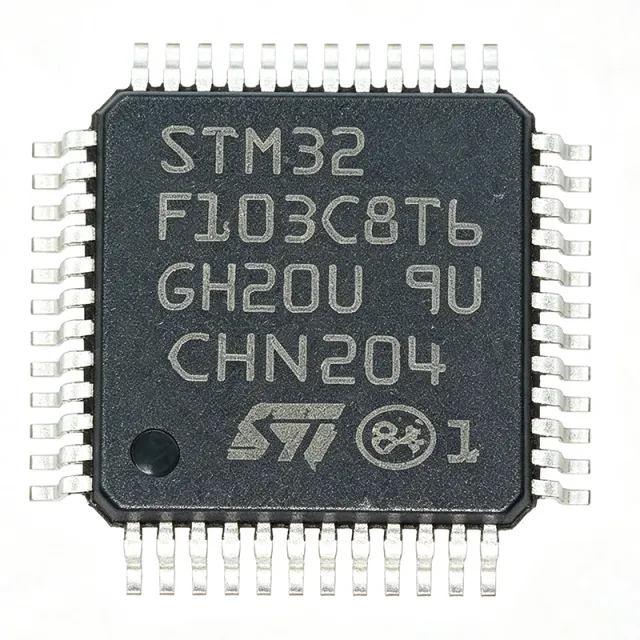
STM32F103C8T6 - 72MHz Cortex-M3 MCU, 64KB Flash | STMicroelectronics
MPN: STM32F103C8T6 ✓ Active| Qty | Unit Price | Extended |
|---|---|---|
| 1 | $4.5 | $4.50 |
| 10 | $4.05 | $40.50 |
| 100 | $3.6 | $360.00 |
| 500 | $3.15 | $1,575.00 |
| 1,000 | $2.8 | $2,800.00 |
STM32F103C8T6 Overview
A microcontroller (MCU) is a single integrated circuit that combines a processor core, memory, and programmable peripherals into one chip, forming the lowest level of the embedded-system hierarchy (MCU -> embedded processor -> system-on-chip). The STM32F1 medium-density performance line sits within STMicroelectronics' broader STM32 family, which spans entry-level Cortex-M0 parts to high-performance Cortex-M7 devices. Medium-density members such as the STM32F103C8 provide the balance of Flash density and peripheral count that made the family an industry standard for cost-sensitive 32-bit control.
Key features include the ARM Cortex-M3 RISC core with 72 MHz maximum frequency, 64 KB embedded Flash and 20 KB SRAM, 37 GPIOs, two 12-bit ADCs with 1 us conversion time, and rich connectivity: 3 USARTs, 2 SPI, 2 I2C, USB 2.0 full-speed, CAN 2.0B, and 6 timers including one advanced PWM timer for motor control. The supply range is 2.0 V to 3.6 V, with dedicated VDDA/VSSA pins isolating analog performance.
Technically, the device connects peripherals across two APB buses with a single-cycle multiply-accumulate DSP-capable core, hardware NVIC with 43 maskable interrupt channels, and power-saving modes (Sleep, Stop, Standby) reaching 2 uA in Standby with the real-time clock running from a 32.768 kHz oscillator.
Typical applications include industrial control, motor drives with 3-phase PWM, IoT sensor nodes using USB or CAN, and the well-known Blue Pill development platform used extensively in education and prototyping.
Design consideration: keep the 3.3 V supply within 2.0-3.6 V, decouple every VDD/VDDA pair with 100 nF plus 4.7 uF bulk capacitance, and verify clock configuration because the core PLL differs between clones and genuine parts.
This page synthesizes verified distributor data, drop-in alternatives including GD32F103C8T6, pinout details, and practical design notes not consolidated in the manufacturer datasheet.
Drop-in alternatives for STM32F103C8T6 — same package, pin-to-pin compatible. Different-package parts requiring PCB rework are excluded.
Variants in this series
Same-series models that are drop-in compatible with STM32F103C8T6 (same form factor and footprint) — differing in Core, Timers, Flash Memory, Package, SRAM.
Quick Comparison Tool — Select alternative parts for side-by-side comparison:
STM32F103CBT6
✅ Drop-In✓ In Stock
$2.4 / Unit
View Datasheet →GD32F103C8T6
✅ Drop-In📋 Reference alternative (not in catalog)
APM32F103C8T6
✅ Drop-In📋 Reference alternative (not in catalog)
AT32F403ACGT7
✅ Drop-In📋 Reference alternative (not in catalog)
STM32G030C8T6
✅ Drop-In✓ In Stock
$1.47 / Unit
View Datasheet →STM32F103C8T6 Maximum Ratings & Electrical Characteristics
| Core | ARM Cortex-M3 32-bit |
| Maximum Clock Frequency | 72 MHz |
| Flash Memory | 64 KB |
| SRAM | 20 KB |
| Supply Voltage | 2.0 V to 3.6 V |
| Number of I/Os | 37 |
| Timers | 6 (3 general-purpose 16-bit, 1 advanced PWM, 1 basic, 1 SysTick) |
| ADC | 2 x 12-bit, 1 us conversion time, 10 channels |
| Communication Interfaces | 3 USART, 2 SPI, 2 I2C, USB 2.0 full-speed, CAN 2.0B |
| DMA Channels | 7 |
| Operating Temperature | -40C to +85C |
| Package | LQFP-48 (7 x 7 mm, 0.5 mm pitch) |
| Mounting Type | Surface Mount |
| Standby Current | 2 uA |
| RoHS Status | Compliant |
| Lifecycle Status | Active |
STM32F103C8T6 Pin Configuration
| Pin 1 | VBAT — Battery backup supply for RTC and backup registers |
| Pin 2 | PC13-TAMPER-RTC — Port C I/O / TAMPER pin / RTC output |
| Pin 3 | PC14-OSC32_IN — Port C I/O / 32 kHz oscillator input |
| Pin 4 | PC15-OSC32_OUT — Port C I/O / 32 kHz oscillator output |
| Pin 5 | PD0-OSC_IN — Port D I/O / main oscillator input |
| Pin 6 | PD1-OSC_OUT — Port D I/O / main oscillator output |
| Pin 7 | NRST — System reset (active low) |
| Pin 8 | VSSA — Analog ground |
| Pin 9 | VDDA — Analog power supply (2.4 V to 3.6 V) |
| Pin 10 | PA0-WKUP — Port A I/O / wakeup / ADC12_IN0 / TIM2_CH1 |
| Pin 11 | PA1 — Port A I/O / ADC12_IN1 / TIM2_CH2 |
| Pin 12 | PA2 — Port A I/O / ADC12_IN2 / USART2_TX / TIM2_CH3 |
| Pin 13 | PA3 — Port A I/O / ADC12_IN3 / USART2_RX / TIM2_CH4 |
| Pin 14 | PA4 — Port A I/O / ADC12_IN4 / SPI1_NSS / DAC out |
| Pin 15 | PA5 — Port A I/O / ADC12_IN5 / SPI1_SCK |
| Pin 16 | PA6 — Port A I/O / ADC12_IN6 / SPI1_MISO |
| Pin 17 | PA7 — Port A I/O / ADC12_IN7 / SPI1_MOSI |
| Pin 18 | PB0 — Port B I/O / ADC12_IN8 / TIM3_CH3 |
| Pin 19 | PB1 — Port B I/O / ADC12_IN9 / TIM3_CH4 |
| Pin 20 | PB2-BOOT1 — Port B I/O / boot pin 1 |
| Pin 21 | PB10 — Port B I/O / I2C2_SCL / USART3_TX / TIM2_CH3 remap |
| Pin 22 | PB11 — Port B I/O / I2C2_SDA / USART3_RX |
| Pin 23 | VSS_1 — Ground |
| Pin 24 | VDD_1 — Digital power supply (2.0 V to 3.6 V) |
| Pin 25 | PB12 — Port B I/O / SPI2_NSS / TIM1_BKIN / USART3_CK |
| Pin 26 | PB13 — Port B I/O / SPI2_SCK / TIM1_CH1N |
| Pin 27 | PB14 — Port B I/O / SPI2_MISO / TIM1_CH2N |
| Pin 28 | PB15 — Port B I/O / SPI2_MOSI / TIM1_CH3N |
| Pin 29 | PA8 — Port A I/O / USART1_CK / TIM1_CH1 / MCO |
| Pin 30 | PA9 — Port A I/O / USART1_TX / TIM1_CH2 |
| Pin 31 | PA10 — Port A I/O / USART1_RX / TIM1_CH3 |
| Pin 32 | PA11 — Port A I/O / USB_DM / CAN_RX / TIM1_CH4 |
| Pin 33 | PA12 — Port A I/O / USB_DP / CAN_TX |
| Pin 34 | PA13-JTMS-SWDIO — Port A I/O / SWD data I/O / JTAG TMS |
| Pin 35 | VSS_2 — Ground |
| Pin 36 | VDD_2 — Digital power supply |
| Pin 37 | PA14-JTCK-SWCLK — Port A I/O / SWD clock / JTAG TCK |
| Pin 38 | PA15-JTDI — Port A I/O / JTDI / SPI1_NSS remap / TIM2_CH1 remap |
| Pin 39 | PB3-JTDO — Port B I/O / JTDO / SPI1_SCK remap / TIM2_CH2 remap |
| Pin 40 | PB4-JTRST — Port B I/O / JTRST / SPI1_MISO remap / TIM3_CH1 remap |
| Pin 41 | PB5 — Port B I/O / I2C1_SMBA / SPI1_MOSI remap / TIM3_CH2 remap |
| Pin 42 | PB6 — Port B I/O / I2C1_SCL / TIM4_CH1 / USART1_TX remap |
| Pin 43 | PB7 — Port B I/O / I2C1_SDA / TIM4_CH2 / USART1_RX remap |
| Pin 44 | BOOT0 — Boot mode selection pin |
| Pin 45 | PB8 — Port B I/O / TIM4_CH3 / CAN_RX remap |
| Pin 46 | PB9 — Port B I/O / TIM4_CH4 / CAN_TX remap |
| Pin 47 | VSS_3 — Ground |
| Pin 48 | VDD_3 — Digital power supply |
Typical Applications
STM32F103C8T6 is suitable for 6 applications: Industrial Control and Automation, Motor Drives and BLDC Control, IoT Sensor Nodes, USB Devices and Peripherals, CAN Bus Networks, Development Boards and Education.
Industrial Control and Automation
The STM32F103C8T6 fits industrial control nodes that need deterministic 32-bit processing, robust communication, and long lifecycle support. Its 72 MHz Cortex-M3 core handles PID loops and protocol stacks simultaneously, while CAN 2.0B and dual USART interfaces connect to PLC backbones and field devices. The -40C to +85C industrial temperature grade and 2.0-3.6 V supply tolerate noisy factory power rails. With 37 GPIOs and 7 DMA channels, the MCU can drive relays, read encoders, and stream sensor data without CPU intervention, keeping interrupt latency predictable via the nested vectored interrupt controller. Typical deployments use a 3.3 V rail with external RS-485 or CAN transceivers, exploiting the F103's mature ST ecosystem and long-standing second-source availability in industrial BOMs.
Recommended
Motor Drives and BLDC Control
The advanced 16-bit timer of the STM32F103C8T6 generates complementary PWM outputs with hardware dead-time insertion, making it a cost-effective controller for 3-phase BLDC and PMSM drives. Its two 12-bit ADCs with 1 us conversion sample phase currents and bus voltage fast enough for field-oriented control at switching frequencies up to 20 kHz, while the 72 MHz core with single-cycle MAC executes FOC loops in software. Sensorless or Hall-based feedback both fit within the 64 KB Flash alongside the control firmware and communication stack. ST publishes motor-control reference designs and libraries targeting this exact family, shortening time to market. Designs requiring higher ADC precision or hardware DSP may step up to the Cortex-M4 based STM32F3 series, but for cost-driven small drives the C8T6 remains a proven choice.
Recommended
IoT Sensor Nodes
For IoT sensor nodes, the STM32F103C8T6 balances processing power against power budget. Sleep, Stop, and Standby modes reduce consumption to 2 uA in Standby with the RTC running from the backup domain on VBAT, enabling years of battery life in duty-cycled designs. The USB 2.0 full-speed peripheral supports direct connection to gateways and configuration tools, while USART, SPI, and I2C link to Wi-Fi, LoRa, or BLE radio modules over standard AT-command or SPI protocols. The 20 KB SRAM comfortably hosts lightweight TCP/MQTT stacks, and the 64 KB Flash leaves room for an in-field bootloader enabling remote firmware updates. Its massive community ecosystem means reference code for virtually every radio module exists, cutting development time significantly for low-volume IoT products.
Recommended
USB Devices and Peripherals
The STM32F103C8T6 integrates a USB 2.0 full-speed device controller, making it a classic choice for HID devices, virtual COM ports, custom bulk-transfer instruments, and USB-to-serial bridges. The 48 MHz USB clock is derived from the external high-speed oscillator through the PLL, ensuring the accuracy USB compliance requires. The 20 KB SRAM provides ample endpoint buffer space, and the 72 MHz core processes protocol layers while concurrently running application logic. ST's USB device library and the enormous community codebase (including virtual-COM-port and HID examples) make bring-up straightforward. Many USB dongles, debug probes, and lab instruments shipped in the last decade are built on exactly this MCU, so interoperability pitfalls are well documented and solved in open-source firmware.
Recommended
CAN Bus Networks
With an integrated bxCAN controller supporting CAN 2.0A/B up to 1 Mbit/s, the STM32F103C8T6 is a mainstay in automotive-adjacent and industrial CAN networks. The controller offers 14 hardware filters and dual FIFOs, offloading frame acceptance from the CPU so the 72 MHz core focuses on application-layer protocols such as CANopen, DeviceNet-style profiles, or OBD-II gateways. Combined with USART and SPI on the same chip, it works well as a protocol translator bridging CAN to Modbus or RS-485 networks. The industrial temperature rating and 5 V-tolerant I/Os ease interfacing with legacy transceivers and sensors. Note that USB and CAN share the SRAM region in this medium-density part, so buffer allocation requires care in designs using both simultaneously.
Recommended
Development Boards and Education
The STM32F103C8T6 is the MCU of the Blue Pill, one of the most distributed development boards ever made, which keeps it central to embedded education and rapid prototyping. Its combination of 72 MHz 32-bit processing, USB, dual ADCs, and sub-dollar clone pricing gives students and engineers a full-featured ARM platform at minimal cost. Toolchain support is exhaustive: STM32CubeIDE, Keil MDK, IAR, PlatformIO, and the Arduino-compatible STM32duino core all target the F103 directly, and ST-Link or serial bootloaders handle programming. For education this means a single inexpensive board teaches C, peripherals, interrupts, RTOS concepts, and USB. For prototyping it means the pinout knowledge and code carry directly into the production LQFP-48 footprint without redesign.
Recommended
Recommended Products Summary
Engineering reference data for STM32F103C8T6 — comparison, design guidance, and compliance information.
Selection Guide
Comparison with Alternatives
| Parameter | This Product | STM32F103CBT6 | GD32F103C8T6 | APM32F103C8T6 | AT32F403ACGT7 |
|---|---|---|---|---|---|
| Package | LQFP-48 (7x7 mm) | LQFP-48 (7x7 mm) - same | LQFP-48 (7x7 mm) - same | LQFP-48 (7x7 mm) - same | LQFP-48 (7x7 mm) - same |
| Brand | STMicroelectronics | STMicroelectronics | GigaDevice | Geehy | Artery Technology |
| Core / Max Frequency | Cortex-M3, 72 MHz | Cortex-M3, 72 MHz | Cortex-M3, 108 MHz | Cortex-M3, 72 MHz | Cortex-M4, up to 200 MHz |
| Flash / SRAM | 64 KB / 20 KB | 128 KB / 20 KB | 64 KB / 20 KB | 64 KB / 20 KB | 256 KB / 96 KB (per variant) |
| USB / CAN | USB 2.0 FS / CAN 2.0B | USB 2.0 FS / CAN 2.0B | USB 2.0 FS / CAN 2.0B | USB 2.0 FS / CAN 2.0B | USB 2.0 FS / CAN 2.0B |
Key Differentiators
- Native ST ecosystem fidelity (vs GD32F103C8T6)
- Cost position vs same-brand memory upgrade (vs STM32F103CBT6)
- 5 V-tolerant I/Os and bxCAN in the base package (vs AT32F403ACGT7)
Design Notes
Decouple every VDD pin (24, 36, 48) with a 100 nF ceramic placed within 3 mm of the pin, plus one 4.7 uF bulk capacitor near the package. Feed VDDA (pin 9) through a ferrite bead from the 3.3 V rail with its own 100 nF plus 1 uF network, because ADC accuracy degrades directly with VDDA ripple. Keep VBAT (pin 1) tied to VDD when no backup battery is used; leaving it floating causes unpredictable RTC and backup-register behavior. Estimated: at 72 MHz full-speed execution, core current is roughly 36-50 mA per ST electrical-characteristics tables, so size the 3.3 V regulator accordingly.
USB requires an exact 48 MHz clock: the internal 8 MHz HSI RC is not accurate enough, so designs using USB must fit an external 8 MHz crystal with correct load capacitors on pins 5 and 6. BOOT0 (pin 44) must be pulled low through a 10 kOhm resistor for normal flash boot; a floating BOOT0 can leave the part in system-bootloader mode and appear 'dead'. Additionally, the F103C8 is the most counterfeited MCU in the market - validate silicon identity (DBGMCU_IDCODE) when sourcing from non-authorized channels, as clones often fail USB compliance and ADC linearity.
For the 7 x 7 mm LQFP-48, connect all three VSS/VDD pin pairs to a solid ground plane via short, low-inductance traces. Route the 8 MHz crystal traces short and symmetric, guarding them with ground. Keep USB D+/D- (PA11/PA12) as a matched 90 Ohm differential pair with 22 Ohm series resistors if traces exceed 30 mm. JTAG/SWD pins (PA13/PA14) should include a 100 nF local decoupling and a 10 kOhm pull-up on SWDIO if long cables or test fixtures connect to them. Exposure of the debug header in production saves rework.
Compliance Information
RoHS compliant per digchip/datasheet data (VFQFPN-48 RoHS compliant notation). REACH and conflict-minerals status not stated in provided data.






