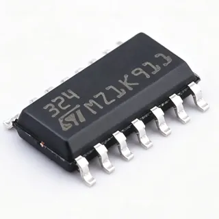
ADL5561ACPZ-R7 - 2.9GHz RF/IF Diff Amp | Analog Devices
MPN: ADL5561ACPZ-R7 ✓ Active| Qty | Unit Price | Extended |
|---|---|---|
| 1 | $13.03 | $13.03 |
| 10 | $12.15 | $121.50 |
| 100 | $10.85 | $1,085.00 |
| 500 | $9.75 | $4,875.00 |
| 1,000 | $8.95 | $8,950.00 |
ADL5561ACPZ-R7 Overview
A differential amplifier is an electronic amplifier that amplifies the difference between two input voltages while rejecting common-mode signals. In RF and IF applications, differential amplifiers are used to convert single-ended signals to differential, drive high-speed ADCs, and provide gain with high linearity. The ADL5561 belongs to the class of RF/IF amplifiers, which are essential in communication systems, radar, and test equipment.
Key features of the ADL5561 include pin-strappable gain adjust of 6 dB, 12 dB, and 15.5 dB, differential or single-ended input to differential output capability, and a low supply current of 40 mA. The amplifier is designed to drive high-speed 8-bit to 16-bit ADCs, providing low noise and high linearity to preserve signal integrity. Its wide bandwidth and low distortion make it ideal for IF sampling receivers, software-defined radios, and broadband communication systems.
The ADL5561 utilizes a differential architecture that provides excellent common-mode rejection and reduces even-order harmonics. The device is specified over a wide temperature range and is RoHS compliant. Its small LFCSP package with exposed pad aids in thermal management, ensuring reliable operation in demanding environments.
Typical applications include ADC drivers for communications and instrumentation, IF amplifier stages in receivers, and differential signal conditioning. The ADL5561 is also suitable for driving mixers and other high-speed analog components.
When designing with the ADL5561, proper layout and decoupling are critical to achieve the specified performance. Use low-inductance capacitors close to the supply pins and maintain a solid ground plane. The exposed pad should be soldered to the PCB ground for optimal thermal and electrical performance.
Drop-in alternatives for ADL5561ACPZ-R7 — same package, pin-to-pin compatible. Different-package parts requiring PCB rework are excluded.
Variants in this series
Same-series models that are drop-in compatible with ADL5561ACPZ-R7 (same form factor and footprint) — differing in Amplifier Type, Package, Slew Rate, Supply Voltage Range, -3 dB Bandwidth.
Quick Comparison Tool — Select alternative parts for side-by-side comparison:
ADL5562ACPZ-R7
✅ Drop-In✓ In Stock
$8.75 / Unit
View Datasheet →ADL5561ACPZ-WP
✅ Drop-In📋 Reference alternative (not in catalog)
ADL5569BCPZ
✅ Drop-In✓ In Stock
$9.28 / Unit
View Datasheet →THS4521
✅ Drop-In ⚠️ Specs Unverified📋 Reference alternative (not in catalog)
LTC6363HMS8-2#PBF
✅ Drop-In ⚠️ Specs Unverified✓ In Stock
$3.75 / Unit
View Datasheet →ADL5561ACPZ-R7 Maximum Ratings & Electrical Characteristics
| Amplifier Type | RF/IF Differential |
| Number of Circuits | 1 |
| -3 dB Bandwidth | 2.9 GHz (AV = 6 dB) |
| Slew Rate | 9800 V/µs |
| Supply Voltage Range | 3 V to 3.6 V |
| Supply Current | 40 mA |
| Input Voltage Noise | 2.1 nV/√Hz |
| Gain Options | 6 dB, 12 dB, 15.5 dB (pin-strappable) |
| Input Configuration | Differential or single-ended |
| Output Configuration | Differential |
| Package / Case | 16-LFCSP-VQ (3x3 mm) |
| Mounting Type | Surface Mount |
| RoHS Status | Compliant |
| Packaging | Tape & Reel (R7) |
ADL5561ACPZ-R7 Pin Configuration
| Pin 1 | VCOM — Output common-mode voltage set |
| Pin 2 | INP — Non-inverting input |
| Pin 3 | INN — Inverting input |
| Pin 4 | VCC — Positive supply |
| Pin 5 | GND — Ground |
| Pin 6 | GND — Ground |
| Pin 7 | OUTP — Non-inverting output |
| Pin 8 | OUTN — Inverting output |
| Pin 9 | GND — Ground |
| Pin 10 | GND — Ground |
| Pin 11 | G1 — Gain select pin 1 |
| Pin 12 | G0 — Gain select pin 0 |
| Pin 13 | VCC — Positive supply |
| Pin 14 | GND — Ground |
| Pin 15 | GND — Ground |
| Pin 16 | VCOM — Output common-mode voltage set |
Typical Applications
ADL5561ACPZ-R7 is suitable for 6 applications: ADC Driver for Communications, IF Amplifier in Receivers, Software-Defined Radio (SDR), Test and Measurement Equipment, Radar and Electronic Warfare, Broadband Communication Systems.
ADC Driver for Communications
The ADL5561ACPZ-R7 is optimized to drive high-speed 8-bit to 16-bit ADCs in communication systems. Its low noise of 2.1 nV/√Hz and high linearity ensure that the ADC receives a clean signal, preserving dynamic range. The wide 2.9 GHz bandwidth supports IF sampling receivers and software-defined radios, where signal integrity is critical. The differential output reduces common-mode noise and even-order harmonics, improving overall system performance. With pin-strappable gains of 6, 12, and 15.5 dB, it can match various ADC input ranges without external components.
Recommended
IF Amplifier in Receivers
In intermediate frequency (IF) stages, the ADL5561ACPZ-R7 provides gain with low distortion, essential for maintaining signal quality in receivers. Its 2.9 GHz bandwidth covers common IF frequencies, and the low noise figure improves receiver sensitivity. The differential architecture rejects common-mode interference, which is beneficial in noisy environments. The device's small LFCSP package allows compact receiver designs, and its low 40 mA supply current reduces power consumption in battery-operated equipment. Pin-strappable gain simplifies gain control without external components.
Recommended
Software-Defined Radio (SDR)
The ADL5561ACPZ-R7 is well-suited for SDR platforms where wideband, low-distortion amplification is required. Its 2.9 GHz bandwidth supports multiple frequency bands, and the low noise of 2.1 nV/√Hz ensures weak signals are not masked. The differential output interfaces directly with differential ADCs, simplifying the signal chain. The device's flexibility in gain settings allows adaptation to different signal levels, and its low power consumption is advantageous for portable SDRs. The compact package enables dense PCB layouts common in SDR designs.
Recommended
Test and Measurement Equipment
In test and measurement instruments, the ADL5561ACPZ-R7 provides accurate signal conditioning for high-speed digitizers. Its low distortion and high bandwidth ensure that measured signals are faithfully reproduced. The differential output reduces noise coupling, which is critical in precision measurements. The device's pin-strappable gain allows easy adjustment for different input ranges, and its small package fits into compact instrument designs. The low supply current helps manage thermal dissipation in densely packed equipment.
Recommended
Radar and Electronic Warfare
The ADL5561ACPZ-R7 is used in radar and electronic warfare systems where wideband, low-noise amplification is essential. Its 2.9 GHz bandwidth covers many radar frequencies, and the low noise figure improves target detection. The differential output provides good common-mode rejection, reducing interference in harsh electromagnetic environments. The device's high linearity minimizes intermodulation distortion, which is critical in multi-signal environments. The compact package and low power consumption are beneficial for airborne and portable systems.
Recommended
Broadband Communication Systems
The ADL5561ACPZ-R7 is ideal for broadband communication systems, including cable modems and fiber-optic receivers. Its wide bandwidth and low distortion support high data rates, while the low noise ensures a high signal-to-noise ratio. The differential output interfaces with differential ADCs, simplifying the receiver chain. The device's gain flexibility allows optimization for various signal levels, and its low power consumption is suitable for customer-premises equipment. The small package enables compact line cards and modems.
Recommended
Recommended Products Summary
Engineering reference data for ADL5561ACPZ-R7 — comparison, design guidance, and compliance information.
Selection Guide
Comparison with Alternatives
| Parameter | This Product | ADL5562ACPZ-R7 | ADL5561ACPZ-WP | THS4521 |
|---|---|---|---|---|
| Package | 16-LFCSP-VQ (3x3 mm) | 16-LFCSP-VQ (3x3 mm) | 16-LFCSP-VQ (3x3 mm) | 16-LFCSP-VQ (3x3 mm) |
| Brand | Analog Devices | Analog Devices | Analog Devices | Texas Instruments |
| Bandwidth | 2.9 GHz | 3.3 GHz | 2.9 GHz | 620 MHz |
| Input Noise | 2.1 nV/√Hz | 2.1 nV/√Hz | 2.1 nV/√Hz | 4.6 nV/√Hz |
| Supply Current | 40 mA | 40 mA | 40 mA | 1.1 mA |
| Supply Voltage | 3 V to 3.6 V | 3 V to 3.6 V | 3 V to 3.6 V | 2.7 V to 5.25 V |
| Gain Options | 6, 12, 15.5 dB | 6, 12, 15.5 dB | 6, 12, 15.5 dB | Adjustable |
| Slew Rate | 9800 V/µs | 9800 V/µs | 9800 V/µs | 740 V/µs |
Key Differentiators
- Wider bandwidth than many alternatives (vs THS4521)
- Lower input noise (vs THS4521)
- Pin-strappable gain without external components (vs THS4521)
Design Notes
For optimal performance, place decoupling capacitors (100 pF and 0.1 µF) as close as possible to the VCC pins. Use a solid ground plane and solder the exposed pad to the PCB ground to enhance thermal and electrical performance. Keep input and output traces short and matched to maintain signal integrity at 2.9 GHz.
Maintain a clean layout with minimal parasitic capacitance on the gain-setting pins (G0, G1). Use via stitching around the ground pads to reduce inductance. For differential signals, ensure symmetrical routing to preserve balance and reduce common-mode noise.
Avoid exceeding the supply voltage range of 3.6 V, as this can damage the device. Ensure the input common-mode voltage is within the specified range to prevent distortion. When using single-ended input, terminate the unused input properly to avoid reflections.
Compliance Information
RoHS compliant per Analog Devices product page. Other compliance data not specified in provided sources.