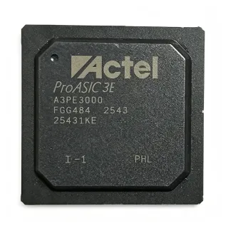
EP4CE15F23C9L - 15,408-Cell 343-I/O Cyclone IV E FPGA | Altera
MPN: EP4CE15F23C9L ✓ ActiveEP4CE15F23C9L Overview
A field-programmable gate array is a semiconductor whose digital logic is configured after manufacture rather than being permanently defined in silicon. The FPGA category sits above programmable logic devices in the broader semiconductor hierarchy and supports parallel architectures, hardware acceleration, interface bridging, and control functions that can be revised without changing the PCB. This flexibility makes an FPGA useful when the final algorithm, interface set, or system partitioning remains under development.
The EP4CE15F23C9L's 15,408 logic cells provide a substantially larger parallel-processing fabric than small programmable logic devices. Its 343 I/O enable direct connections to external memory, sensors, converters, communications transceivers, and control signals. The F23 device uses a 484-ball FBGA package, requiring careful escape-routing, via density, and thermal management on multilayer PCB designs. The ball-pitch dimensions and exposed-package thermal characteristics should be confirmed from the package drawings before layout release.
Programmable systems typically use the Cyclone IV E logic fabric for datapath acceleration, interface control, protocol conversion, and supervisory logic. Because FPGA designs depend on timing constraints, pin assignments, device configuration, and tool-supported memory interfaces, designers should use the Quartus design software version supported for the Cyclone IV E device family. Configuration flash, clocks, resets, power sequencing, and JTAG access require careful planning for reliable field operation.
Thermal performance depends on the selected speed grade, core voltage, utilization, toggle rate, and PCB copper. The manufacturer package drawing should be used to determine land geometry, ball assignments, and exposed thermal-pad requirements. Signal-integrity analysis is particularly important for high-speed memory interfaces, and the board should maintain continuous return paths beneath high-speed routing.
This page consolidates the exact package and ordering information for EP4CE15F23C9L, compares same-package Cyclone IV E options, and identifies practical design checks that are not apparent from a distributor summary. It also explains where to obtain the official ordering-part-number page, how to evaluate a replacement, and which information must be confirmed before committing a new PCB.
Drop-in alternatives for EP4CE15F23C9L — same package, pin-to-pin compatible. Different-package parts requiring PCB rework are excluded.
Variants in this series
Same-series models that are drop-in compatible with EP4CE15F23C9L (same form factor and footprint) — differing in Process Technology, Configuration Modes, Logic Elements, Package, Speed Grade.
EP4CE15F23I8L
✅ Drop-InContact for price
View Datasheet →EP4CE15F23C7N
✅ Drop-In ⚠️ Specs UnverifiedContact for price
View Datasheet →EP4CE15F23C8N
✅ Drop-In ⚠️ Specs UnverifiedContact for price
View Datasheet →EP4CE15F23I7N
✅ Drop-In ⚠️ Specs Unverified📋 Reference alternative (not in catalog)
EP4CE40F23A7N
✅ Drop-InContact for price
View Datasheet →EP4CE15F23C9L Maximum Ratings & Electrical Characteristics
| Device Type | FPGA |
| FPGA Family | Cyclone IV E |
| Device Designation | EP4CE15 |
| Package Configuration | F23 |
| Logic Cells | 15,408 cells |
| I/O Count | 343 I/O |
| Process Technology | 60 nm |
| Core Supply Voltage | 1.2 V |
| Package Type | 484-FBGA |
| Package Ball Count | 484 balls |
| Terminal Form | Ball |
| Package Shape | Square |
| Mounting Type | Surface Mount |
EP4CE15F23C9L square Pin Configuration Guide
Pin configuration for EP4CE15F23C9L (square package). This digital IC includes GPIO, communication interfaces (UART, SPI, I2C), and power pins. Refer to the manufacturer datasheet for alternate pin functions and configuration options. Essential for embedded system design and PCB layout.

No detailed pinout data available for EP4CE15F23C9L.
Refer to the datasheet for full pin configuration.
Typical Applications
EP4CE15F23C9L is suitable for 6 applications: Industrial Control and Automation, Video and Image Processing, Industrial Networking and Protocol Bridging, Data Acquisition and Signal Conditioning, Test and Measurement Systems, Secure Embedded and Cryptographic Control.
Industrial Control and Automation
The EP4CE15F23C9L fits centralized machine-control logic because its 15,408 logic cells can implement multiple state machines, interlocks, sequencing logic, and peripheral-control functions in parallel. Its 343 I/O provide substantial connectivity for digital sensors, actuators, encoders, and industrial interface circuits. The 484-ball FBGA also supports dense multilayer routing for communications and memory interfaces. Before deployment, confirm the exact temperature range, speed grade, power behavior, and lifecycle requirements. The control design should also include watchdogs, fail-safe outputs, configuration fault handling, and isolation appropriate to the machine environment.
Recommended
Video and Image Processing
The EP4CE15F23C9L can implement parallel pixel pipelines, color-space conversion, frame timing, test-pattern generation, and interface-format conversion because 15,408 logic cells are suited to deterministic parallel operations rather than sequential software execution. Its 343 I/O can connect image sensors, frame buffers, and parallel display interfaces, subject to supported device I/O standards and timing constraints. The dense 484-ball FBGA makes short escape routes practical on a multilayer board. Designers should constrain clock domains carefully, validate memory timing in the supported Quartus tool flow, and reserve logic and routing resources for timing closure.
Recommended
Industrial Networking and Protocol Bridging
EP4CE15F23C9L is suitable for fixed-format protocol conversion, packet filtering, and interface isolation because its programmable parallel fabric can implement multiple data paths and finite-state machines at deterministic clock rates. The 343 available I/O give designers room to bridge parallel buses, memory interfaces, and industry-specific links without relying on a large external ASIC. Because Cyclone IV E I/O performance depends on the selected bank, voltage, and standards configuration, engineers must review device support and timing constraints. PCB signal integrity, clock jitter, and termination schemes should be evaluated for each high-speed channel.
Recommended
Data Acquisition and Signal Conditioning
The EP4CE15F23C9L can implement parallel acquisition control, digital filtering, calibration tables, trigger logic, and data packing around external converters. Its 15,408-cell fabric supports concurrent pipelines while its 343 I/O allow direct connection to multi-channel converter buses and memory devices. This makes the FPGA useful when deterministic sampling sequences and flexible post-processing must coexist. Designers should verify converter interface timing against the selected Cyclone IV E speed grade and I/O-bank requirements. Add clock-cleaning, isolation, and thermal monitoring to preserve measurement integrity in precision or high-channel-count systems.
Recommended
Test and Measurement Systems
EP4CE15F23C9L is well matched to programmable test logic, sequencing engines, pattern generation, acquisition control, and real-time analysis because the parallel fabric can run multiple deterministic channels concurrently. The 343 I/O supports dense connections to instruments, DUT interfaces, relays, and memory resources. A 484-ball package leaves little board-routing margin, so power, ground, test-point access, and debug routing should be planned early. For production test equipment, the design should include boundary-scan or JTAG access, deterministic reset, safe configuration loading, and fault containment around DUT control lines.
Recommended
Secure Embedded and Cryptographic Control
EP4CE15F23C9L can implement parallel cryptographic engines, authentication control, protocol firewalls, and key-handling state machines within a programmable embedded platform. Its 15,408 logic cells allow independent pipelines to operate concurrently, while 343 I/O provide access to external nonvolatile storage and communication devices. Security design must still include a protected boot process, authenticated configuration, secure key storage, fault detection, and resistance to fault injection. The exact configuration method and security features must be confirmed for the selected Cyclone IV E device and tool flow before the design is treated as production-ready.
Recommended
Recommended Products Summary
Engineering reference data for EP4CE15F23C9L — comparison, design guidance, and compliance information.
Selection Guide
Comparison with Alternatives
| Parameter | This Product | EP4CE15F23I8L | EP4CE15F23C7N | EP4CE15F23C8N | EP4CE15F23I7N | EP4CE40F23A7N |
|---|---|---|---|---|---|---|
| Brand | Altera | Altera | Altera | Altera | Altera | Altera |
| Package | 484-FBGA | 484-FBGA - same | 484-FBGA - same | 484-FBGA - same | 484-FBGA - same | 484-FBGA - same |
| Process Technology | 60 nm | 60 nm | 60 nm | 60 nm | 60 nm | 60 nm |
| Core Supply Voltage | 1.2 V | 1.2 V | 1.2 V | 1.2 V | 1.2 V | 1.2 V |
| Ordering Suffix | C9L | I8L | C7N | C8N | I7N | A7N |
Key Differentiators
- Provides the same 15,408-cell resource level as the closest EP4CE15F23 ordering variants (vs EP4CE15F23I8L)
- Keeps the dense 484-ball FBGA footprint across the listed F23 alternatives (vs EP4CE40F23A7N)
- Targets the EP4CE15 capacity class rather than the larger EP4CE40 device (vs EP4CE40F23A7N)
Design Notes
Treat the 484-ball FBGA as a multilayer-board design rather than a conventional two-layer routing exercise. Follow the manufacturer package drawing for ball pitch, solder-mask definition, land geometry, and thermal-pad construction. Provide uninterrupted core and I/O supply planes, adequate decoupling at each power ball group, and a low-impedance ground reference directly beneath the FPGA. Escape-routing density and via access should be checked against every assigned power, ground, configuration, clock, and user signal before layout release.
FPGA junction temperature depends on core voltage, speed grade, logic utilization, switching activity, and board heat spreading. Use the manufacturer power-estimation methodology with the expected clocking, utilization, and environmental temperature rather than applying a generic thermal margin. Preserve the package's specified copper and via pattern around exposed thermal features, minimize thermal vias beneath sensitive routes where required, and use a multilayer board with generous ground copper. Validate the final assembly at the highest expected activity and ambient temperature.
Assign external memories and high-speed interfaces only after checking the Cyclone IV E I/O standards, supported data rates, bank voltage limits, and available clocking resources. Keep traces short, provide continuous reference planes, and use manufacturer-recommended termination for each interface class. Avoid switching voltage or clock domains directly between unrelated banks. External clock jitter and board skew must be included in timing closure, particularly when the FPGA coordinates parallel acquisition, video, or packet-processing paths.
A compatible package outline does not by itself authorize a suffix substitution. Verify the ordering code, temperature grade, speed grade, supply limits, configuration interface, exposed-pad details, and revision-specific differences in the manufacturer documentation. Also confirm that the Quartus tool version supports the selected OPN. After changing EP4CE15F23C9L to another suffix, rerun synthesis, place-and-route, timing analysis, and bitstream-generation checks rather than assuming that only the ordering label changed.
Compliance Information
The device is an industrial FPGA rather than an automotive-qualified AEC-Q100 option. RoHS, REACH, lead-free, halogen-free, and conflict-minerals status require confirmation from the current manufacturer product documentation.