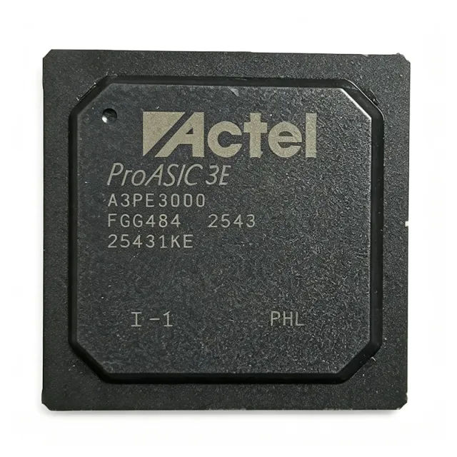
A3P600-FGG484I - 600K Gate Flash FPGA, 231MHz | Microchip
MPN: A3P600-FGG484I ✓ Active| Qty | Unit Price | Extended |
|---|---|---|
| 1 | $86.5 | $86.50 |
| 10 | $78.2 | $782.00 |
| 100 | $69.8 | $6,980.00 |
| 500 | $62.5 | $31,250.00 |
| 1,000 | $55.3 | $55,300.00 |
A3P600-FGG484I Overview
A field programmable gate array (FPGA) is a semiconductor device containing programmable logic blocks and programmable interconnect that can be configured after manufacturing to implement custom digital logic. The A3P600-FGG484I belongs to the ProASIC3 family, which uses flash-based configuration cells instead of SRAM. This places it within the broader FPGA hierarchy: flash FPGA -> ProASIC3 family -> Microchip programmable logic portfolio. Because configuration is stored in non-volatile flash, the device is instantly live on power-up, requires no external boot PROM, and resists unauthorized readback, making it suitable for secure and mission-critical systems.
Key features of the A3P600-FGG484I include 600K system gates, 235 user I/O, 13.5 kB SRAM, 231 MHz system performance, and a 1.5 V core supply. The flash-based architecture provides instant-on operation, low power, and single-chip security. The FGG484 package is a lead-free 484-ball fine-pitch ball grid array, and the industrial temperature grade supports applications from -40C to +100C (per Microchip's standard industrial-grade definition). The device is programmable through a standard JTAG interface and can be reprogrammed in-system for prototyping or field updates.
The ProASIC3 architecture uses 130 nm flash technology, balancing density, performance, and cost. Since configuration is stored on-chip, external configuration memory is eliminated, reducing BOM cost and board space while improving security. The device supports multiple I/O standards, enabling direct interface to LVCMOS, LVTTL, and other common logic families. The 13.5 kB SRAM can be used for FIFOs, small buffers, or scratchpad memory in soft-processor and state-machine designs, and the 231 MHz system performance is adequate for many industrial, communications, and display processing tasks.
Typical applications include industrial motor control, avionics display processing, medical monitoring, communications protocol bridging, and IoT edge aggregation. The instant-on behavior and secure flash configuration make the A3P600-FGG484I a strong choice for security-conscious designs such as encrypted communication modules and tamper-resistant control systems. The 235 I/O pins support parallel data buses, memory interfaces, and high-density sensor arrays, and the 1.5 V core reduces power consumption compared to older 3.3 V FPGAs.
When designing with the A3P600-FGG484I, pay attention to power-supply decoupling and I/O bank planning. Place 100 nF ceramic capacitors close to each power/ground ball pair and use bulk capacitance on the 1.5 V core rail. Verify that each I/O bank voltage is connected to the correct external supply before configuration, and leave unused I/O in a defined state. Because the device is flash-based, no configuration device is required, but a JTAG header is recommended for programming and debug. Follow Microchip's PCB layout guidance for the 484-ball FBGA to ensure reliable solder joints and thermal performance.
This page synthesizes distributor pricing, same-family drop-in alternatives, and practical design notes not found in the manufacturer datasheet, helping engineers select, validate, and replace the A3P600-FGG484I with confidence.
Drop-in alternatives for A3P600-FGG484I — same package, pin-to-pin compatible. Different-package parts requiring PCB rework are excluded.
Variants in this series
Same-series models that are drop-in compatible with A3P600-FGG484I (same form factor and footprint) — differing in Package, Core Supply Voltage, RoHS Status, Configuration, Process Technology.
Quick Comparison Tool — Select alternative parts for side-by-side comparison:
A3P600-2FGG484I
✓ In Stock
$31.8 / Unit
View Datasheet →A3P600-1FGG484I
✓ In Stock
$79.6 / Unit
View Datasheet →A3P600-FGG484
✓ In Stock
$44.75 / Unit
View Datasheet →A3P600-2FGG484I
✓ In Stock
$31.8 / Unit
View Datasheet →A3P600-1FGG484
✓ In Stock
$52.4 / Unit
View Datasheet →A3P600L-FGG484I
✓ In Stock
$41.35 / Unit
View Datasheet →A3P600-FGG484I Maximum Ratings & Electrical Characteristics
| FPGA Family | ProASIC3 |
| System Gates | 600000 |
| Number of User I/O | 235 |
| Embedded SRAM | 13.5 kB |
| System Performance | 231 MHz |
| Process Technology | 130 nm |
| Core Supply Voltage | 1.5 V |
| Package Type | 484-FBGA |
| Mounting Type | Surface Mount |
| Operating Temperature Grade | Industrial (I suffix) |
| Lead-Free Finish | Yes (LEAD FREE per Mouser listing) |
| Configuration | Flash-based, non-volatile, instant on |
| Programming Interface | JTAG |
| AEC-Q100 | Not applicable (FPGA) |
| Tray Packaging | Yes (per datasheets.com listing) |
A3P600-FGG484I 484-fbga Pin Configuration Guide
Pin configuration for A3P600-FGG484I (484-fbga package). This digital IC includes GPIO, communication interfaces (UART, SPI, I2C), and power pins. Refer to the manufacturer datasheet for alternate pin functions and configuration options. Essential for embedded system design and PCB layout.

No detailed pinout data available for A3P600-FGG484I.
Refer to the datasheet for full pin configuration.
Typical Applications
A3P600-FGG484I is suitable for 6 applications: Industrial Motor Control, Avionics Display Processing, Medical Monitoring Equipment, Communications Protocol Bridging, IoT Edge Aggregation, Secure Instant-On System Logic.
Industrial Motor Control
The A3P600-FGG484I is well suited for industrial motor control because its 600K system gates can implement multiple encoder interfaces, PWM generation, and protection logic in parallel, while its 231 MHz performance keeps loop timing deterministic. The 1.5 V flash FPGA consumes less power than older 3.3 V PLDs, simplifying thermal design in sealed control cabinets. The instant-on characteristic is valuable in safety-related motor drives where the controller must begin monitoring the power stage immediately after power-up. With 235 user I/O, the FPGA can connect to resolver interfaces, Hall sensors, current-sense ADCs, and a host microcontroller. In this application, the FPGA handles high-speed commutation logic while an external MCU such as the TMS320F28027FPTT executes the motor-control algorithm. The non-volatile configuration also avoids the risk of a missing configuration file after a brownout.
Recommended
Avionics Display Processing
The A3P600-FGG484I is used in avionics display processing because it can bridge multiple video and sensor buses while providing deterministic timing and secure bitstream storage. The industrial temperature grade supports the extended environmental ranges found in unpressurized avionics bays, and the flash-based instant-on behavior ensures the display logic is active as soon as power is applied. With 235 I/O, the device can connect to LVDS receivers, character displays, and backlight controllers. The 13.5 kB embedded SRAM provides small line buffers for video scan conversion or icon overlay generation. The non-volatile flash configuration prevents bitstream tampering, which is a concern in safety-certified avionics systems. For lower-power avionics line-replaceable units, the A3P600L-FGG484I variant is worth evaluating; however, the standard A3P600-FGG484I provides the best balance of density and performance for mid-range display processing tasks.
Recommended
Medical Monitoring Equipment
The A3P600-FGG484I fits medical monitoring equipment because it can aggregate and preprocess multiple physiological sensor channels with low latency. Its 235 user I/O allow direct connection to ADC outputs, digital pulse-oximeter front-ends, and serial sensor buses, while the flash-based architecture uses non-volatile configuration for reliable instant-on in critical care devices. The 13.5 kB embedded SRAM can serve as a FIFO for data streaming or as a small buffer for waveform scaling. The industrial temperature grade gives margin for the self-heating inside sealed medical enclosures. In a typical patient-monitor subsystem, the FPGA performs data alignment, filtering, and alarm logic, while an MSP430FR5994 microcontroller handles communication, display, and user interface. The low power of the 1.5 V core helps medical devices meet stringent energy-efficiency standards and simplifies thermal management in compact housings.
Recommended
Communications Protocol Bridging
The A3P600-FGG484I is effective as a communications protocol bridge because it can handle multiple serial protocols in parallel while maintaining the required 231 MHz data path throughput. The 484-FBGA package provides ample I/O for connecting to UARTs, SPI, I2C, and parallel host ports, and the 13.5 kB SRAM can buffer packets between dissimilar interfaces. Because the FPGA is flash-based, the bridging logic is available immediately at power-up, eliminating the boot delay seen with SRAM FPGAs. This is important in network switches, industrial gateways, and protocol converters where the bridge must forward data within a strict latency budget. The non-volatile configuration also protects intellectual property in deployed edge devices. For designs that need a host CPU for management and queuing, the MSP430FR5994 can supervise the FPGA and handle upper-layer protocol processing, while the FPGA maintains real-time data movement.
Recommended
IoT Edge Aggregation
The A3P600-FGG484I is a good fit for IoT edge aggregation because it can collect data from multiple sensors and preprocess it before forwarding to a host processor or radio, reducing the computational load on the main MCU. The instant-on flash configuration is valuable in battery-powered edge nodes because the FPGA can begin collecting data immediately after a wake event without waiting for configuration loading. The 1.5 V core and 130 nm process deliver acceptable power for many outdoor IoT gateways, and the 235 I/O enable connection to a wide range of digital sensors, switch matrices, and level translators. In an edge aggregator, the FPGA can combine UART streams, debounce contact closures, and timestamp events, while an MSP430FR5994 or CC430F5145 handles wireless transmission and power management. The secure flash configuration also helps prevent overbuilding or unauthorized cloning of IoT hardware.
Recommended
Secure Instant-On System Logic
The A3P600-FGG484I is ideal for secure instant-on system logic because its flash-based configuration starts executing immediately and cannot be externally read back, protecting the programmed bitstream. In security systems such as access controllers, surveillance preprocessors, and encryption bridges, the FPGA can implement watchdog logic, tamper detection, and secure state machines without depending on an external configuration PROM. The 600K gates provide room for cryptographic helper functions or data obfuscation, while the 13.5 kB SRAM buffers small key or status tables. The industrial temperature grade supports outdoor camera housings and unattended installations. For system-level security, pair the FPGA with a TPD4S012DRYR protection device on exposed I/O and an MSP430FR5994 for secure key management. The non-volatile instant-on behavior also ensures no unconfigured window during which an attacker could manipulate the logic.
Recommended
Recommended Products Summary
Engineering reference data for A3P600-FGG484I — comparison, design guidance, and compliance information.
Selection Guide
Comparison with Alternatives
| Parameter | This Product | A3P600-2FGG484I | A3P600-1FGG484I | A3P600-FGG484 | A3P600-2FGG484 | A3P600-1FGG484 | A3P600L-FGG484I |
|---|---|---|---|---|---|---|---|
| Package | 484-FBGA | 484-FBGA | 484-FBGA | 484-FBGA | 484-FBGA | 484-FBGA | 484-FBGA |
| Brand | Microchip Technology | Microchip Technology | Microchip Technology | Microchip Technology | Microchip Technology | Microchip Technology | Microchip Technology |
| FPGA Family | ProASIC3 | ProASIC3 | ProASIC3 | ProASIC3 | ProASIC3 | ProASIC3 | ProASIC3L |
| System Gates | 600000 | 600000 | 600000 | 600000 | 600000 | 600000 | 600000 |
| Core Supply Voltage | 1.5 V | 1.5 V | 1.5 V | 1.5 V | 1.5 V | 1.5 V | 1.5 V |
| User I/O Count | 235 | 235 | 235 | 235 | 235 | 235 | 235 |
| Embedded SRAM | 13.5 kB | 13.5 kB | 13.5 kB | 13.5 kB | 13.5 kB | 13.5 kB | 13.5 kB |
| Operating Temperature Grade | Industrial (I suffix) | Industrial | Industrial | Commercial | Commercial | Commercial | Industrial |
Key Differentiators
- Industrial temperature grade enabled by the I suffix (vs A3P600-FGG484)
- Standard speed grade balances cost and performance (vs A3P600-2FGG484I)
- Wide availability through multiple distribution channels (vs A3P600L-FGG484I)
Design Notes
The A3P600-FGG484I operates from a 1.5 V core supply. Place a 100 nF ceramic capacitor close to each core power ball and add bulk capacitance (10 uF or greater) at the power entry point. According to Microchip's ProASIC3 datasheet DS50003269, all power supplies should be clean and properly decoupled to achieve rated performance. Estimated: a 231 MHz design with moderate I/O activity can draw a few hundred milliamperes from the 1.5 V rail; size the regulator to support the transient current indicated in the datasheet electrical characteristics.
For the 484-ball FBGA, use a high-layer-count PCB with dedicated power and ground planes under the device. Follow Microchip's layout guidelines for ball escape routing and thermal pad connection. The fine-pitch BGA requires accurate solder mask registration and controlled impedance if used with high-speed I/O. Add a JTAG header for programming and boundary-scan testing, and consider series termination resistors on clock and high-speed outputs. Use the manufacturer design resources and IBIS models to simulate signal integrity for critical nets.
Because the A3P600-FGG484I is flash-based, it does not require an external configuration PROM, but the JTAG interface must be accessible for programming and debug. Do not leave the 1.5 V core supply unregulated or exceed the absolute maximum ratings listed in the datasheet. Unused user I/O should be configured to a defined state to avoid floating inputs and excessive supply current. If migrating from A3P600-FGG484 to A3P600-2FGG484I, re-verify timing closure for the higher speed grade, even though the pinout is identical.
Compliance Information
Lead-free status is indicated by the 'LEAD FREE' label in the Mouser listing. RoHS/REACH specific statements were not provided in the verified web data and are marked unknown until confirmed from the manufacturer datasheet or certificate.
