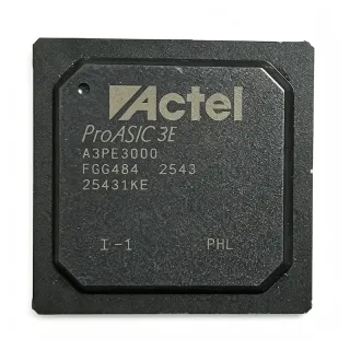
A3P1000-1FGG484T - Automotive ProASIC3 FPGA | Microchip
MPN: A3P1000-1FGG484T ✓ Active| Qty | Unit Price | Extended |
|---|---|---|
| 1 | $48.3 | $48.30 |
| 10 | $43.7 | $437.00 |
| 100 | $39.5 | $3,950.00 |
| 500 | $36.8 | $18,400.00 |
| 1,000 | $33.9 | $33,900.00 |
A3P1000-1FGG484T Overview
A field-programmable gate array is an integrated circuit whose logic fabric can be configured after manufacturing, allowing designers to implement custom digital hardware without a custom ASIC. Unlike microcontrollers, FPGAs execute parallel hardware datapaths with deterministic timing. ProASIC3 is Microchip's flash-based FPGA family, providing non-volatile configuration, instant-on operation, and a single-chip solution with no external boot PROM. In the power management and embedded processing hierarchy, this device sits at the programmable-logic layer, complementing MCUs, DSPs, and ASSPs in mixed-signal systems.
Key features of the A3P1000-1FGG484T include 1M system gates, 11K logic elements, 300 user I/Os, 147,456 bits of RAM, 272 MHz system performance, and a 1.5 V core supply. The device is qualified to AEC-Q100, making it suitable for automotive electronics. The 484-ball FBGA package provides a high-density interconnect for complex board-level routing. The flash-based architecture gives instant-on capability and intrinsic design security.
Architecturally, ProASIC3 devices use a 130 nm flash CMOS process. The flash cells act as both configuration memory and logic switches, eliminating the need for external configuration devices. This reduces system cost and PCB area while improving security against IP cloning. The VersaTile-based fabric implements combinatorial and sequential logic efficiently. The 300 user I/Os support multiple I/O standards, enabling flexible interfacing to sensors, memories, and communication transceivers.
Typical applications include automotive ADAS and infotainment, industrial motor control and factory automation, communications and networking equipment, medical imaging, and aerospace mission systems. For automotive use, the AEC-Q100 qualification and 1M-gate density allow integration of pre-processing and safety logic. In industrial designs, the 300 I/OS and flash instant-on provide reliable, low-latency control.
When designing with this FPGA, ensure the 1.5 V core supply is well decoupled with 0.1 uF and 1 uF ceramic capacitors close to each supply ball. Use thermal vias under the BGA to reduce junction temperature. Because the device is flash-based, no external boot PROM is required; however, JTAG programming and in-system reconfiguration should be planned in the schematic.
This page synthesizes distributor pricing, drop-in alternatives, and practical design notes not found in the manufacturer datasheet, giving engineers a single reference for sourcing, replacement, and board bring-up.
Drop-in alternatives for A3P1000-1FGG484T — same package, pin-to-pin compatible. Different-package parts requiring PCB rework are excluded.
Variants in this series
Same-series models that are drop-in compatible with A3P1000-1FGG484T (same form factor and footprint) — differing in Family, System Gates, Core Voltage, Operating Temperature, Package.
Quick Comparison Tool — Select alternative parts for side-by-side comparison:
A3P1000-1FG484T
✅ Drop-In ⚠️ Specs Unverified✓ In Stock
$160 / Unit
View Datasheet →A3P1000-FGG484T
✅ Drop-In📋 Reference alternative (not in catalog)
A3P1000-2FGG484M
✅ Drop-In ⚠️ Specs Unverified✓ In Stock
$75.44 / Unit
View Datasheet →A3P1000-FG484I
✅ Drop-In📋 Reference alternative (not in catalog)
A3P1000L-1FGG484I
✅ Drop-In ⚠️ Specs Unverified✓ In Stock
$28.8 / Unit
View Datasheet →A3P1000-1FGG484T Maximum Ratings & Electrical Characteristics
| Category | FPGA - Field Programmable Gate Array |
| Series | ProASIC3 |
| System Gates | 1M |
| Logic Elements | 11K |
| Total RAM Bits | 147456 |
| Number of User I/O | 300 |
| Core Supply Voltage | 1.5 V |
| Maximum Operating Frequency | 272 MHz |
| Technology Node | 130 nm CMOS |
| Package / Case | 484-FBGA |
| Number of Pins | 484 |
| Ball Pitch | 0.80 mm |
| Mounting Type | Surface Mount |
| Automotive Grade | AEC-Q100 Qualified |
| Configuration | Flash-based |
A3P1000-1FGG484T 484-fbga Pin Configuration Guide
Pin configuration for A3P1000-1FGG484T (484-fbga package). This digital IC includes GPIO, communication interfaces (UART, SPI, I2C), and power pins. Refer to the manufacturer datasheet for alternate pin functions and configuration options. Essential for embedded system design and PCB layout.

No detailed pinout data available for A3P1000-1FGG484T.
Refer to the datasheet for full pin configuration.
Typical Applications
A3P1000-1FGG484T is suitable for 6 applications: Automotive ADAS and Infotainment, Industrial Motor Control and Factory Automation, Aerospace and Mission Computing, Communications and Networking Equipment, Medical Imaging and Patient Monitoring, IoT Edge and Smart Sensor Hubs.
Automotive ADAS and Infotainment
The A3P1000-1FGG484T is AEC-Q100 qualified, making it suitable for automotive ADAS pre-processing, sensor fusion, and infotainment bridge logic. Its 1M system gates and 300 user I/Os can implement camera interface timing, CAN/LIN protocol bridges, and display control logic at 1.5 V core. The flash-based fabric keeps an instantaneous configuration state during power-up, supporting safe power sequencing in automotive modules. With 272 MHz performance, it handles high-speed datapath tasks such as image cropping and pixel formatting while offloading the main SoC. Designers should verify I/O standard compatibility with the automotive transceivers and use the 484-FBGA package for dense routing in multilayer automotive PCBs.
Recommended
Industrial Motor Control and Factory Automation
In industrial motor control, the A3P1000-1FGG484T provides flexible logic for PWM generation, encoder decoding, and safety interlocking. Its 300 user I/Os allow direct connection to gate drivers, position sensors, and industrial fieldbus PHYs. The 147,456 bits of RAM are useful for small FIFOs and parameter tables in real-time control loops. The instant-on flash configuration ensures the FPGA starts in a known state without waiting for an external configuration memory, which is important for safety-rated systems. The 484-FBGA package supports high pin-count interfaces to multiple incremental encoders and parallel data buses. While an external MCU or DSP handles high-level control loops, the FPGA implements cycle-accurate I/O timing with low latency.
Recommended
Aerospace and Mission Computing
The flash-based A3P1000-1FGG484T offers single-chip, non-volatile operation ideal for aerospace payload controllers and mission data handling. Unlike SRAM-based FPGAs, it does not require external configuration PROMs, reducing board space and potential single points of failure. With 1M gates and 300 I/Os, it can interface with radiation-hardened companion devices, sensor front-ends, and telemetry links. The 272 MHz performance supports high-rate data multiplexing and protocol encoding. Although this specific package is not a hermetic space-grade package, its industrial/automotive temperature variants can be screened for high-reliability commercial aerospace. Engineers should follow derating guidelines for power, temperature, and I/O stress in mission profiles.
Recommended
Communications and Networking Equipment
The A3P1000-1FGG484T is used in communications line cards, small switches, and protocol converters. Its 300 I/Os can implement parallel buses to Ethernet PHYs, SERDES, or memory devices. The 147,456 bits of RAM provide FIFO buffering for packet queues, while the 1M-gate fabric can handle framing, CRC, and statistical multiplexing functions. Flash-based configuration makes the FPGA immediately available after power-on, reducing network equipment boot time. The 130 nm process with 1.5 V core balances speed and power for 272 MHz logic. For 10/100 Ethernet bridging, the FPGA can implement MAC/PHY glue logic without an external CPU, though more complex switching generally requires an external network processor.
Recommended
Medical Imaging and Patient Monitoring
For ultrasound beamforming, CT data pre-processing, and patient monitoring front-ends, the A3P1000-1FGG484T offers deterministic parallel processing with 300 I/Os. The 147,456 bits of RAM support line buffers and coefficient tables, while the 1M-gate fabric can implement digital filters and correlation engines. The AEC-Q100 qualification, while aimed at automotive, also indicates strong reliability for medical equipment. Designers can use the flash-based instant-on feature to ensure the device is ready quickly for safety-critical monitoring. The 1.5 V core and 272 MHz performance support moderate throughput imaging tasks. EMI considerations are important in medical environments; use proper decoupling and controlled impedance routing on the 484-FBGA breakout.
Recommended
IoT Edge and Smart Sensor Hubs
The A3P1000-1FGG484T can serve as an edge sensor hub, aggregating data from multiple sensors and implementing custom protocols before forwarding to an MCU or cloud gateway. Its 300 I/Os allow connection to many sensor channels, ADCs, and communication interfaces. The flash-based fabric provides instant-on and secure boot, important for unattended IoT devices. The 147,456 bits of RAM enable small data buffering, and the 1M-gate fabric can implement hardware acceleration for sensor fusion math. While the 484-FBGA package is larger than typical IoT MCUs, the FPGA is well suited for industrial IoT gateways and smart building controllers where deterministic, low-latency sensor processing is required. Power consumption can be optimized with the low-power A3P1000L variant.
Recommended
Recommended Products Summary
Engineering reference data for A3P1000-1FGG484T — comparison, design guidance, and compliance information.
Selection Guide
Comparison with Alternatives
| Parameter | This Product | A3P1000-1FG484T | A3P1000-FGG484T | A3P1000-2FGG484M | A3P1000-FG484I | A3P1000L-1FGG484I |
|---|---|---|---|---|---|---|
| Package | 484-FBGA | 484-FBGA | 484-FBGA | 484-FBGA | 484-FBGA | 484-FBGA |
| Brand | Microchip Technology | Microchip Technology | Microchip Technology | Microchip Technology | Microchip Technology | Microchip Technology |
| Logic Elements | 11K | 11K | 11K | 11K | 11K | 11K |
| System Gates | 1M | 1M | 1M | 1M | 1M | 1M |
| Number of User I/O | 300 | 300 | 300 | 300 | 300 | 300 |
| Core Supply Voltage | 1.5 V | 1.5 V | 1.5 V | 1.5 V | 1.5 V | 1.2 V |
| Speed Grade | -1 | -1 | default | -2 | default | -1 |
Key Differentiators
- AEC-Q100 qualified automotive FPGA (vs A3P1000-FG484I)
- Flash-based instant-on single-chip operation (vs SRAM-based competitor FPGAs)
- 1M system gates and 300 user I/Os in 484-FBGA (vs A3P1000L-1FGG484I)
Design Notes
The A3P1000-1FGG484T core operates from a 1.5 V supply. Place a 0.1 uF ceramic capacitor close to each core supply ball and a bulk 1 uF capacitor per quadrant. Estimated core current can be 200-500 mA depending on design utilization and switching frequency. Use a low-noise LDO or switching regulator with adequate headroom; verify the 1.5 V rail tolerance with the FPGA power calculator in Libero SoC.
The 484-FBGA package has a small footprint for 1M gates; thermal management is important. Estimated power dissipation at 272 MHz with 60% logic utilization and 50% I/O toggle is approximately 1.5-3 W. Use a 4-layer or higher PCB with thermal vias in the center pad of the BGA to an internal ground plane to help conduct heat. Consider airflow if the device is in a sealed enclosure.
Because ProASIC3 is flash-based, it is non-volatile and does not need an external configuration PROM. Do not forget to connect the JTAG pins and provide a programming interface. In multi-rail systems, ensure the 1.5 V core powers up within the specified ramp rate and that I/O banks are not driven before the core supply is valid. Refer to the Microchip ProASIC3 FPGA datasheet for pin-specific power-up requirements.
Compliance Information
AEC-Q100 qualification is stated in the DigiKey listing. The 'G' in the part number typically indicates a green package, but RoHS/REACH/lead-free status is not explicitly stated in the verified web data and should be confirmed with Microchip documentation.