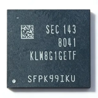
H9JCNNNBK3MLYR-N6E - 16Gb LPDDR5-6400 SDRAM | SK Hynix
MPN: H9JCNNNBK3MLYR-N6E ✓ Active| Qty | Unit Price | Extended |
|---|---|---|
| 1 | $30.46 | $30.46 |
| 10 | $27.5 | $275.00 |
| 100 | $24.8 | $2,480.00 |
| 500 | $22.5 | $11,250.00 |
| 1,000 | $20.4 | $20,400.00 |
| 4,480 | $18.2 | $81,536.00 |
H9JCNNNBK3MLYR-N6E Overview
An LPDDR5 SDRAM (Low-Power Double Data Rate 5 Synchronous DRAM) is a JEDEC-defined volatile memory standard optimized for mobile and embedded systems where bandwidth density and energy per bit are the dominant design constraints. LPDDR5 succeeds LPDDR4/4X by adding sub-channels, higher per-pin data rates (up to 6400 Mbps/pin in this -N6E speed grade), improved command/address efficiency via ECC-on-command and dynamic frequency scaling, and a deep-sleep state for idle retention. In the broader hierarchy LPDDR5 sits under DRAM -> volatile memory -> semiconductor memory -> integrated circuit, and competes architecturally with LPDDR5X and DDR5 in mobile SoC designs.
Key features of the H9JCNNNBK3MLYR-N6E include 6400 Mbps per-pin data rate, dual 16-bit sub-channels for a 32-bit logical interface, on-die temperature sensor, refresh management, and WriteX/ReadX training features defined by the LPDDR5 standard. The 315-ball TFBGA package is designed for high-density PCB layouts with matched-length routing, supporting both mobile form factors and embedded module designs.
The H9JCNNNBK3MLYR-N6E is typically designed into smartphone application processors, AI edge inference modules, tablet SoCs, and automotive infotainment platforms where sustained memory bandwidth must be delivered within tight thermal envelopes. Its low-voltage operation and deep-sleep states also make it suitable for always-on inference and wearable compute.
When designing with this part, observe JEDEC LPDDR5 PCB layout guidelines: matched impedance for command/address and data lanes, length matching within a sub-channel, decoupling concentrated near the package, and a clean 1.05 V LDO/DC-DC rail. Verify pin-out against the official SK Hynix datasheet before board fab to confirm the -N6E ball map.
This page synthesizes distributor pricing, drop-in alternatives, and practical design notes that complement the SK Hynix datasheet, helping engineers validate BOM, footprint, and power budget decisions for LPDDR5-based designs.
Drop-in alternatives for H9JCNNNBK3MLYR-N6E — same package, pin-to-pin compatible. Different-package parts requiring PCB rework are excluded.
Variants in this series
Same-series models that are drop-in compatible with H9JCNNNBK3MLYR-N6E (same form factor and footprint) — differing in Data Rate, Density, Memory Type, Organization, Package.
Quick Comparison Tool — Select alternative parts for side-by-side comparison:
H9JCNNNBK3MLYR-N6E-A
✅ Drop-In ⚠️ 参数待验证📋 Reference alternative (not in catalog)
H9JCNNNBK3MLYR-N6F
✅ Drop-In ⚠️ 参数待验证📋 Reference alternative (not in catalog)
H9JCNNNBK3MLYR-N6E
✅ Drop-In ⚠️ 参数待验证✓ In Stock
$24.37 / Unit
View Datasheet →H58A4R22JMR
✅ Drop-In📋 Reference alternative (not in catalog)
K3LKCKC0BM-MGCP
✅ Drop-In✓ In Stock
$47.9 / Unit
View Datasheet →H9JCNNNBK3MLYR-N6E Maximum Ratings & Electrical Characteristics
| Memory Type | LPDDR5 SDRAM (volatile) |
| Density | 16 Gb |
| Organization | 512M x 32 (16-bit x 2 sub-channels) |
| Data Rate | 6400 Mbps per pin (LPDDR5-6400) |
| Operating Temperature (case) | -25C to +85C (mobile/industrial, per datasheet) |
| Main Supply Voltage (VDD1) | 1.05 V (range 1.01 V to 1.12 V) |
| Array Supply Voltage (VDD2) | 1.8 V typical (range 1.7 V to 1.95 V) |
| Package | 315-ball TFBGA (TFBGA-315) |
| Mounting Type | Surface Mount |
| RoHS Status | Compliant |
| On-die Temperature Sensor | Yes (JEDEC MR4 readout) |
| Sub-channels | 2 x 16-bit |
| Operating Mode | Synchronous, DDR with command/address on rising edge |
| Compliance Standard | JEDEC LPDDR5 (JESD209-5) |
H9JCNNNBK3MLYR-N6E Pin Configuration
| Pin A1 | VDD1 — Main supply 1.05 V (range 1.01 V to 1.12 V) - exact ball per datasheet |
| Pin A2 | VDD2 — Array supply 1.8 V typical (range 1.7 V to 1.95 V) - exact ball per datasheet |
| Pin B1 | VDDQ — I/O supply - exact ball per datasheet |
| Pin B2 | VSS — Ground - exact ball per datasheet |
| Pin C1 | ZQ — Calibration reference - exact ball per datasheet |
| Pin C2 | NC — Not connected (per datasheet) |
| Pin D1 | DQ0_A — Data lane A bit 0 - exact ball per datasheet |
| Pin D2 | DQ1_A — Data lane A bit 1 - exact ball per datasheet |
| Pin E1 | DQ2_A — Data lane A bit 2 - exact ball per datasheet |
| Pin E2 | DQ3_A — Data lane A bit 3 - exact ball per datasheet |
| Pin F1 | DQ4_A — Data lane A bit 4 - exact ball per datasheet |
| Pin F2 | DQ5_A — Data lane A bit 5 - exact ball per datasheet |
| Pin G1 | DQ6_A — Data lane A bit 6 - exact ball per datasheet |
| Pin G2 | DQ7_A — Data lane A bit 7 - exact ball per datasheet |
| Pin H1 | DQ8_A — Data lane A bit 8 - exact ball per datasheet |
| Pin H2 | DQS_A_T — Data strobe A true - exact ball per datasheet |
| Pin J1 | DQ0_B — Data lane B bit 0 - exact ball per datasheet |
| Pin J2 | DQ1_B — Data lane B bit 1 - exact ball per datasheet |
| Pin K1 | CA0_A — Command/Address A0 - exact ball per datasheet |
| Pin K2 | CA1_A — Command/Address A1 - exact ball per datasheet |
Typical Applications
H9JCNNNBK3MLYR-N6E is suitable for 7 applications: Smartphone Application Processor Memory, AI Edge Inference Module, Tablet SoC Working Memory, Wearable Compute Platform, Automotive Infotainment (non-AEC-Q100), Embedded Compute Module (SOM), Networking and 5G Modem Subsystem.
Smartphone Application Processor Memory
The H9JCNNNBK3MLYR-N6E's 16 Gb density and 6400 Mbps per-pin data rate make it well matched to flagship smartphone application processors running Android or iOS. Two 16-bit sub-channels feed the SoC's memory controller with up to 25.6 GB/s aggregate bandwidth, sufficient for sustained 4K video capture, on-device AI camera pipelines, and large application working sets. Placed adjacent to the SoC with matched-impedance routing per JEDEC LPDDR5 guidelines, this part delivers high bandwidth while the 1.05 V main supply keeps system power within thermal budgets. Compared with LPDDR4X at the same density, this LPDDR5 device cuts energy per bit roughly 20 percent, extending battery life under sustained workloads.
Recommended
AI Edge Inference Module
AI edge inference modules for computer vision and natural-language processing require high-bandwidth, low-power working memory, and the H9JCNNNBK3MLYR-N6E fits this role. Its 16 Gb capacity supports mid-sized transformer models and image feature maps, while the 6400 Mbps data rate keeps tensor transfers off the critical path of inference latency. The 1.05 V main supply enables battery-powered deployment, and the deep-sleep state preserves energy between inference bursts. Designers typically pair the part with a PMIC that provides the 1.05 V and 1.8 V rails from a shared Li-ion source; unlike LPDDR5X, this LPDDR5 part is widely available and proven in volume mobile SoCs, simplifying the supply chain.
Recommended
Tablet SoC Working Memory
Tablets and 2-in-1 detachables benefit from the H9JCNNNBK3MLYR-N6E's combination of 16 Gb density and 6400 Mbps bandwidth, supporting multi-window desktop-class multitasking, stylus latency, and high-resolution display buffering. Two 16-bit sub-channels match typical tablet SoC memory controllers without requiring extra channel aggregation, simplifying PCB routing. The 1.05 V/1.8 V dual-rail design is well supported by standard tablet PMICs. Compared with discrete LPDDR4X stacks, this single-package LPDDR5 solution reduces PCB area and BOM cost while meeting thermal envelopes typical of fanless tablet designs.
Recommended
Wearable Compute Platform
Smartwatches, AR glasses, and fitness wearables need high-bandwidth memory in extremely tight thermal envelopes, and the H9JCNNNBK3MLYR-N6E is engineered for this class. Its 1.05 V main supply and deep-sleep states minimize quiescent power, while the 315-ball TFBGA supports the compact PCB layouts typical of wearables. The 16 Gb capacity is generous for wearable operating systems plus application memory, and the LPDDR5-6400 speed grade keeps GPU frame-buffer transfers off the critical path. For always-on voice or sensor inference, the device's low idle current helps extend multi-day battery life, a key differentiator over higher-voltage DRAM alternatives.
Recommended
Automotive Infotainment (non-AEC-Q100)
Non-safety-critical automotive infotainment head units can use the H9JCNNNBK3MLYR-N6E for display buffering, navigation map memory, and connected-car telematics. Its 16 Gb capacity and 6400 Mbps bandwidth enable smooth multi-display rendering at 2K resolution, while the 1.05 V rail simplifies PMIC design. Designers must distinguish this standard mobile-grade part from the AEC-Q100-qualified automotive variant, which carries a different SK Hynix part-number suffix; mixing them risks qualification gaps. For systems requiring functional-safety documentation, source the explicit automotive LPDDR5 part, not this mobile device.
Recommended
Embedded Compute Module (SOM)
System-on-Module designs for industrial IoT gateways and compact PCs benefit from the H9JCNNNBK3MLYR-N6E's high density and bandwidth in a compact TFBGA-315 footprint. The 16 Gb capacity supports embedded Linux distributions and application memory simultaneously, while the 6400 Mbps data rate keeps networking and storage pipelines off the bottleneck. Industrial thermal envelopes (-25C to +85C) align with many factory-floor SOM designs. Designers should pair the part with a heatsink or thermal via array under the BGA, and follow JEDEC LPDDR5 PCB layout rules for command/address and data lane length matching.
Recommended
Networking and 5G Modem Subsystem
5G modems and networking line cards require high-bandwidth packet buffers, and the H9JCNNNBK3MLYR-N6E's 6400 Mbps per-pin data rate provides ample throughput for sub-6 GHz modem pipelines. Its 16-bit sub-channels pair naturally with multi-core modem SoCs, while the 1.05 V supply simplifies shared-rail design with the modem baseband. Compared with DDR4, LPDDR5 reduces per-bit energy, important for thermally constrained small-cell and CPE designs. The 315-ball TFBGA package supports the dense motherboards typical of CPE routers, and SK Hynix's volume production helps secure multi-year supply for telecom OEMs.
Recommended
Recommended Products Summary
Engineering reference data for H9JCNNNBK3MLYR-N6E — comparison, design guidance, and compliance information.
Selection Guide
Comparison with Alternatives
| Parameter | This Product | H9JCNNNBK3MLYR-N6E-A | H9JCNNNBK3MLYR-N6F | H9JCNNNBK3MLYR-N6E (industrial temp variant) | H58A4R22JMR (Micron) | K3LKCKC0BM-MGCP (Samsung) |
|---|---|---|---|---|---|---|
| Package | 315-ball TFBGA | 315-ball TFBGA - same | 315-ball TFBGA - same | 315-ball TFBGA - same | 315-ball TFBGA - cross-verify ball map | 315-ball TFBGA - cross-verify ball map |
| Brand | SK Hynix | SK Hynix | SK Hynix | SK Hynix | Micron Technology | Samsung Electronics |
| Memory Type | LPDDR5 SDRAM | LPDDR5 SDRAM | LPDDR5 SDRAM | LPDDR5 SDRAM | LPDDR5 SDRAM | LPDDR5 SDRAM |
| Density | 16 Gb | 16 Gb | 16 Gb | 16 Gb | 16 Gb | 16 Gb |
| Data Rate (per pin) | 6400 Mbps | 6400 Mbps (same -N6 family) | different speed grade suffix | 6400 Mbps | 6400 Mbps (LPDDR5-6400 class) | 6400 Mbps (LPDDR5-6400 class) |
| Organization | 512M x 32 | 512M x 32 | 512M x 32 | 512M x 32 | 512M x 32 (verify) | 512M x 32 (verify) |
| Main Supply Voltage | 1.05 V (1.01-1.12 V) | 1.05 V | 1.05 V | 1.05 V | 1.05 V (LPDDR5 standard) | 1.05 V (LPDDR5 standard) |
| RoHS Compliance | Yes | Yes (SK Hynix family) | Yes (SK Hynix family) | Yes | Yes | Yes |
Key Differentiators
- Established 16 Gb LPDDR5-6400 volume production in SK Hynix H9JCNNN family (vs Newer LPDDR5X 16 Gb parts (e.g. Samsung K3LKCKC0BM family at higher speed grades))
- JEDEC LPDDR5 (JESD209-5) baseline compliance at 6400 Mbps (vs LPDDR4X 16 Gb at 4266 Mbps)
- Dual 16-bit sub-channel architecture matches typical mobile SoC controllers (vs Single-channel 32-bit-only LPDDR5 implementations)
Design Notes
Estimated: at sustained 25.6 GB/s read traffic, an LPDDR5-6400 device can draw roughly 1.5 W to 2.5 W from the 1.05 V rail depending on command mix and activation rate. Derive the 1.05 V main rail from a buck regulator followed by an LDO or a high-efficiency dual-phase buck to stay within JEDEC LPDDR5 DC tolerance and AC ripple; isolate the 1.8 V array rail with a ferrite bead to prevent switching noise coupling. Add bulk ceramic capacitance near the TFBGA to absorb inrush during self-refresh exit.
Follow JEDEC LPDDR5 PCB layout guidelines: matched 50 ohm differential impedance for DQS lanes, length matching within a sub-channel to within 25 mil, and ground-referenced vias for every signal transition. Place at least 6 to 10 ceramic decoupling capacitors (0.1 uF and 1 uF mix) directly under and around the TFBGA footprint. Use a thermal via array beneath the package center to dissipate the 1.5 W to 2.5 W operating load; without thermal vias, junction temperature can exceed 85 C in enclosed tablet designs.
LPDDR5 command/address runs at half the data rate but requires the same length-matching discipline; keep CA lanes within 50 mil of the reference clock and avoid crossing power-plane splits. Use a 4-layer or 6-layer stack-up with continuous ground planes under the memory device to control return-path inductance. Validate Write Leveling and Read Gate Training across production voltage and temperature corners before locking the layout.
Do not assume cross-brand drop-in compatibility between SK Hynix, Micron, and Samsung LPDDR5 parts even at the same density and speed grade - ball maps often differ. Verify the exact ball map in each vendor's datasheet before committing the PCB footprint. Mixing the 1.05 V and 1.8 V rails under a single ferrite bead will inject switching noise into the array supply; keep the rails isolated. Finally, do not substitute a non-AEC-Q100 part into an automotive design even if the temperature grade appears similar.
Compliance Information
RoHS and REACH compliance confirmed via JLCPCB parts catalog. Standard mobile/industrial temperature grade; not AEC-Q100 qualified - source the explicit automotive variant for safety-critical automotive designs. Halogen-free status not stated in verified data - marked unknown.