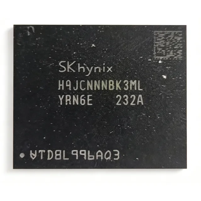
H9JCNNNBK3MLYR-N6E - 16Gb LPDDR5-6400 SDRAM | SK Hynix
MPN: H9JCNNNBK3MLYR-N6E ✓ Active| Qty | Unit Price | Extended |
|---|---|---|
| 1 | $30.46 | $30.46 |
| 10 | $28.94 | $289.40 |
| 100 | $27.41 | $2,741.00 |
| 500 | $25.89 | $12,945.00 |
| 1,000 | $24.37 | $24,370.00 |
H9JCNNNBK3MLYR-N6E Overview
LPDDR5 (Low-Power Double Data Rate 5) is the fifth generation of the JEDEC low-power DRAM standard, positioned above LPDDR4X in the memory hierarchy: LPDDR5 SDRAM -> low-power DRAM -> DRAM -> volatile memory IC. Unlike standard DDR5 DIMM modules, LPDDR5 devices are soldered directly to the PCB, use a narrow 32-bit (x32) channel, and trade socketability for dramatically lower I/O power and a smaller footprint. The 1.05 V VDD2 rail is lower than the 1.1 V of LPDDR4X, which is the primary lever for reducing total memory power in battery-operated systems.
Key differentiators of this part include its 6400 Mbps pin speed (a 33% uplift over LPDDR4X-4266), the 512M x 32 organization that maps cleanly onto 32-bit SoC memory controllers, and the TFBGA-315 ballout that is footprint-compatible across the SK Hynix LPDDR5 family. The device supports bank-group architecture and a low-power clock-stop mode for aggressive idle power reduction.
Architecturally, the die uses SK Hynix's advanced 1-alpha-class DRAM process and integrates on-die termination (ODT), a programmable write-leveling scheme, and per-bank refresh to reduce peak current. The dual-channel x16+x16 internal split allows the controller to interleave accesses and hide refresh latency, which is critical for sustained bandwidth in AI inference and 4K video pipelines.
Typical applications include flagship smartphones, automotive ADAS domain controllers, edge AI inference modules, 5G CPE and small cells, AR/VR headsets, and industrial machine-vision systems. In each case the 6400 Mbps rate and 1.05 V rail allow the SoC to hit its memory-bandwidth target without a discrete power penalty.
A key design consideration is that LPDDR5 requires careful PCB trace-length matching and impedance control on the 32-bit data bus; unlike a DIMM, there is no module-level calibration, so signal integrity must be engineered at the board level. This page synthesizes distributor pricing, drop-in alternatives, and practical design notes not found in the manufacturer datasheet.
Drop-in alternatives for H9JCNNNBK3MLYR-N6E — same package, pin-to-pin compatible. Different-package parts requiring PCB rework are excluded.
Quick Comparison Tool — Select alternative parts for side-by-side comparison:
H9JCNNNBK3MLYR-N6E-SK
✓ In Stock
$20.85 / Unit
View Datasheet →H9JCNNNBK3MLYR-N6E
✓ In Stock
$18.2 / Unit
View Datasheet →H9JCNNNBK3MLYR-N6E Maximum Ratings & Electrical Characteristics
| Memory Type | LPDDR5 SDRAM |
| Density | 16 Gb (2 GB) |
| Organization | 512M x 32 |
| Data Rate | 6400 Mbps per pin |
| Supply Voltage (VDD2) | 1.05 V |
| Package | TFBGA-315 |
| Mounting Type | Surface Mount |
| Number of Channels | Dual channel (x16 + x16) |
| RoHS Status | Compliant |
| Memory Technology | DRAM (volatile) |
H9JCNNNBK3MLYR-N6E tfbga-315 Pin Configuration Guide
Pin configuration for H9JCNNNBK3MLYR-N6E (tfbga-315 package). This digital IC includes GPIO, communication interfaces (UART, SPI, I2C), and power pins. Refer to the manufacturer datasheet for alternate pin functions and configuration options. Essential for embedded system design and PCB layout.

No detailed pinout data available for H9JCNNNBK3MLYR-N6E.
Refer to the datasheet for full pin configuration.
Typical Applications
H9JCNNNBK3MLYR-N6E is suitable for 6 applications: Flagship Smartphone Memory, Automotive ADAS Domain Controller, Edge AI Inference Module, 5G CPE and Small Cell, AR/VR Headset, Industrial Machine Vision.
Flagship Smartphone Memory
The H9JCNNNBK3MLYR-N6E fits flagship smartphone designs because its 6400 Mbps per-pin rate and 512M x 32 organization give a 32-bit SoC memory controller roughly 25.6 GB/s of peak bandwidth, enough for 4K video capture and on-device AI inference. The 1.05 V VDD2 rail is lower than LPDDR4X's 1.1 V, directly extending battery life in always-on workloads. The device is soldered directly to the main PCB in a 315-ball TFBGA, so there is no module socket and no DIMM calibration step; the phone maker must instead engineer trace-length matching and impedance control on the 32-bit bus. A typical implementation pairs the part with a mobile SoC and a PMIC that sequences the VDD1, VDD2, and VDDQ rails during boot.
Recommended
Automotive ADAS Domain Controller
ADAS domain controllers need deterministic, high-bandwidth memory for sensor fusion and neural-network inference, and the H9JCNNNBK3MLYR-N6E supplies 6400 Mbps per pin across a 32-bit channel for exactly this workload. The 16 Gb density is sufficient to hold multiple camera frames plus model weights, while the 1.05 V rail keeps the module inside the thermal budget of a sealed automotive enclosure. Because the part is a soldered TFBGA-315 rather than a socketed module, it survives the vibration and thermal cycling of under-hood and cabin-mounted ECUs. Designers should confirm the temperature grade and AEC-Q100 status in the SK Hynix datasheet, since the available distributor data does not state an automotive qualification for this specific ordering code.
Recommended
Edge AI Inference Module
Edge AI inference modules are bandwidth-bound, and the H9JCNNNBK3MLYR-N6E's 6400 Mbps pin rate delivers the memory throughput needed to keep an NPU fed without stalling on weight fetches. The 512M x 32 organization maps cleanly onto the 32-bit memory controllers common in edge SoCs, and the dual-channel x16+x16 internal split lets the controller interleave accesses to hide refresh latency. At 1.05 V VDD2 the device also keeps the module's idle power low enough for fanless operation. A typical design places the part adjacent to the SoC with matched-length traces and a shared PMIC rail, and relies on the LPDDR5 clock-stop mode to cut power between inference bursts.
Recommended
5G CPE and Small Cell
5G CPE and small-cell baseband units buffer large numbers of packets and run real-time scheduling, so they need low-latency, high-bandwidth DRAM. The H9JCNNNBK3MLYR-N6E provides 6400 Mbps per pin over a 32-bit channel, which is enough to sustain multi-gigabit throughput without dropping packets during buffer bursts. The 16 Gb density accommodates packet buffers, control-plane state, and firmware in a single device, simplifying the BOM. Because the part is a 315-ball TFBGA, it mounts on the same board as the baseband SoC and RF front end, and the 1.05 V rail reduces the power drawn from the CPE's DC supply. Trace-length matching on the 32-bit bus remains the critical layout task.
Recommended
AR/VR Headset
AR/VR headsets are extremely power- and weight-sensitive, and the H9JCNNNBK3MLYR-N6E addresses both constraints: its 1.05 V VDD2 rail lowers memory power versus LPDDR4X, and its 315-ball TFBGA footprint is small enough for a compact headset mainboard. The 6400 Mbps pin rate supports the high refresh rates and stereo rendering pipelines that headsets require, while the 16 Gb density holds frame buffers and tracking data. Because the device is soldered rather than socketed, it also tolerates the mechanical shock of head movement. Designers typically pair it with a low-power SoC and a PMIC that sequences the three LPDDR5 rails, and must control impedance on the short, dense 32-bit bus.
Recommended
Industrial Machine Vision
Industrial machine-vision systems capture high-resolution frames at high frame rates and must process them in real time, which makes memory bandwidth the limiting factor. The H9JCNNNBK3MLYR-N6E supplies 6400 Mbps per pin across a 32-bit channel, enough to stream multiple camera feeds into an FPGA or vision SoC without frame drops. The 16 Gb density holds several full-resolution frames plus algorithm state, and the soldered TFBGA-315 package resists the vibration present on production lines. The 1.05 V rail also helps keep the vision module within a fanless thermal envelope. A typical design places the DRAM close to the vision processor with matched trace lengths and a dedicated PMIC rail for the LPDDR5 supplies.
Recommended
Engineering reference data for H9JCNNNBK3MLYR-N6E — comparison, design guidance, and compliance information.
Selection Guide
Comparison with Alternatives
| Parameter | This Product | H9JCNNNBK3MLYR-N6E | H9JCNNNBK3MLYR-N6E (Tray) | H9JCNNNBK3MLYR-N6E (Reel) |
|---|---|---|---|---|
| Package | TFBGA-315 | TFBGA-315 - same | TFBGA-315 - same | TFBGA-315 - same |
| Brand | SK Hynix | SK Hynix | SK Hynix | SK Hynix |
| Density | 16 Gb (2 GB) | 16 Gb | 16 Gb | 16 Gb |
| Organization | 512M x 32 | 512M x 32 | 512M x 32 | 512M x 32 |
| Data Rate | 6400 Mbps | 6400 Mbps | 6400 Mbps | 6400 Mbps |
| VDD2 Supply | 1.05 V | 1.05 V | 1.05 V | 1.05 V |
| Memory Technology | LPDDR5 SDRAM | LPDDR5 SDRAM | LPDDR5 SDRAM | LPDDR5 SDRAM |
| RoHS | Compliant | Compliant | Compliant | Compliant |
| Mounting Type | Surface Mount | Surface Mount | Surface Mount | Surface Mount |
Key Differentiators
- 6400 Mbps pin rate versus LPDDR4X-4266 (vs LPDDR4X-4266 equivalent)
- 1.05 V VDD2 rail versus 1.1 V LPDDR4X (vs LPDDR4X-4266 equivalent)
- 512M x 32 organization for 32-bit controllers (vs x16 LPDDR5 devices)
- TFBGA-315 family-standard ballout (vs non-family LPDDR5 packages)
Design Notes
LPDDR5 has no module-level calibration, so the 32-bit data bus must be length-matched at the board level. Keep all DQ, DQS, and DMI traces within a tight skew budget (typically a few mils) and route them over a continuous reference plane. Use the TFBGA-315 ballout from the SK Hynix LPDDR5 datasheet to assign byte lanes, and verify that each byte lane's DQS pair is matched to its eight DQ lines before releasing the layout.
The H9JCNNNBK3MLYR-N6E uses a 1.05 V VDD2 core rail, lower than the 1.1 V of LPDDR4X. Sequence VDD1, VDD2, and VDDQ in the order specified by the SK Hynix datasheet and hold the rails within tolerance during boot, because LPDDR5 mode-register initialization is sensitive to rail order. Decouple each rail with low-ESR ceramic capacitors placed close to the TFBGA-315 power balls.
Estimated: at 6400 Mbps the device's I/O power scales with data rate and bus utilization, so sustained full-bandwidth traffic raises the die temperature above idle. Provide a thermal path from the TFBGA-315 package to the PCB ground plane through the ball array, and avoid placing the DRAM directly under a heat-generating SoC. Confirm the actual junction-temperature limit and thermal resistance in the SK Hynix datasheet, since the available distributor data does not state them.
Do not assume a cross-brand LPDDR5 part is pin-compatible with the H9JCNNNBK3MLYR-N6E. Although JEDEC standardizes the LPDDR5 protocol, ballouts and mode-register defaults can differ between vendors, and a mismatch can prevent the SoC from completing memory training. Always compare the full 315-ball map and the initialization sequence before substituting a different manufacturer's device.
Compliance Information
Distributor listings (JLCPCB, LCSC) state ROHS compliance for the H9JCNNNBK3MLYR-N6E. REACH, lead-free, halogen-free, conflict-minerals, and AEC-Q100 status are not stated in the available data and must be confirmed with SK Hynix.