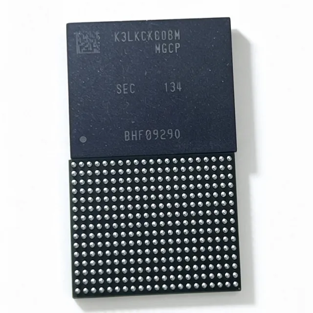
K3LKCKC0BM-MGCP - 64Gb LPDDR5 SDRAM 6400 Mbps | Samsung
MPN: K3LKCKC0BM-MGCP ✓ Active| Qty | Unit Price | Extended |
|---|---|---|
| 1 | $112.5 | $112.50 |
| 10 | $81.25 | $812.50 |
| 100 | $71.875 | $7,187.50 |
| 500 | $68.75 | $34,375.00 |
| 1,000 | $65.625 | $65,625.00 |
K3LKCKC0BM-MGCP Overview
LPDDR5 (Low Power Double Data Rate 5) is a JEDEC-defined CMOS DRAM memory technology optimized for mobile and power-sensitive computing. In the memory hierarchy it sits as the main system DRAM below the CPU/SoC cache, providing high-bandwidth working memory with aggressive power management such as deep power-down, DVFS, and bank group architectures.
Key features include 64 Gbit density in a single package, 6400 Mbps data rate (equivalent to 51.2 GB/s aggregate bandwidth in a x32 dual-channel system as promoted on the Samsung LPDDR5 product page), low-voltage signaling for reduced power, and RoHS compliance. The x32 organization supports burst-oriented, channel-interleaved access typical of application processors.
Architecturally, the device uses a CMOS DRAM core with LPDDR5 bank-group structure, on-die termination, and speed-grade optioning encoded in the MPN suffix. The MGCP suffix denotes package/speed binning per Samsung ordering information.
Typical applications include flagship smartphone main memory, automotive infotainment and ADAS edge-computing SoCs, and AI edge modules where high bandwidth-per-watt is critical.
Design consideration: the memory controller and PCB routing must support 6400 Mbps signaling; impedance control, fly-by termination, and per-rail decoupling of the 1.05V/1.8V/900mV/500mV supplies are essential for signal integrity.
This page adds value beyond the datasheet by consolidating distributor stock and pricing data, drop-in family alternatives, and practical design notes in one place.
Drop-in alternatives for K3LKCKC0BM-MGCP — same package, pin-to-pin compatible. Different-package parts requiring PCB rework are excluded.
Variants in this series
Same-series models that are drop-in compatible with K3LKCKC0BM-MGCP (same form factor and footprint) — differing in Package, Density, Interface, Memory Type, Organization.
Quick Comparison Tool — Select alternative parts for side-by-side comparison:
K3LKBKB0BM-MGCP
✓ In Stock
$46.62 / Unit
View Datasheet →K3LKCKC0BM-MGCP Specifications
| Memory Type | LPDDR5 SDRAM |
| Density | 64 Gbit (8 GB) |
| Organization | 2G x32 |
| Data Rate | 6400 Mbps |
| Interface | CMOS, LPDDR5 |
| Supply Voltage (VDD1) | 1.05 V |
| Supply Voltage (VDD2/other rails) | 1.8 V, 900 mV, 500 mV |
| Operating Temperature | -25C to +85C |
| Package | FBGA-315 (PBGA) |
| Mounting Type | Surface Mount |
| RoHS Status | Compliant |
| Technology | CMOS DRAM |
| Product Family | Samsung LPDDR5 |
| Bandwidth (per Samsung LPDDR5 family) | 51.2 GB/s (family-level, 6400 Mbps pin speed) |
| Power Saving (family feature) | Up to 20% power saving vs previous generation (Samsung LPDDR5 family) |
| Unit Price | USD 57.7195 (LCSC, as of 2026-09-04) |
K3LKCKC0BM-MGCP fbga-315 (pbga) Pin Configuration Guide
Pin configuration for K3LKCKC0BM-MGCP (fbga-315 (pbga) package). Pin numbering, functions, and connection diagrams are defined in the manufacturer datasheet. Refer to it for the exact footprint and soldering guidelines.

No detailed pinout data available for K3LKCKC0BM-MGCP.
Refer to the datasheet for full pin configuration.
Typical Applications
K3LKCKC0BM-MGCP is suitable for 6 applications: Flagship Smartphone Main Memory, Automotive Infotainment and Cockpit SoCs, Industrial Edge-AI Computing Modules, 5G Networking and Edge Servers, Mobile AI Accelerators and NPUs, High-End Consumer Electronics and Tablets.
Flagship Smartphone Main Memory
The K3LKCKC0BM-MGCP is designed as main system DRAM for flagship smartphones, where its 64 Gbit (8 GB) capacity and 6400 Mbps pin speed feed high-resolution camera pipelines, on-device AI inference, and multitasking workloads. Samsung states its LPDDR5 family achieves 51.2 GB/s aggregate bandwidth and roughly 20% power savings versus the previous generation, which directly extends battery life in the SoC's dominant power consumer after the CPU. The multi-rail architecture (1.05V, 1.8V, 900mV, 500mV) integrates with application-processor PMICs, and the -25C to +85C rating covers typical mobile thermal envelopes. Placement close to the SoC (Package-on-Package or PoP-near layouts) minimizes trace length at 6400 Mbps, preserving signal integrity across the x32 data bus.
Recommended
Automotive Infotainment and Cockpit SoCs
Automotive cockpit and infotainment platforms increasingly use LPDDR5 to drive multi-display clusters, 3D navigation, and voice assistants. The K3LKCKC0BM-MGCP's -25C to +85C operating range suits cabin electronics, and its 6400 Mbps data rate supplies the bandwidth needed for high-resolution HMI rendering from an automotive-grade SoC. Distributor listings (AB Sunshine, JLCPCB) identify this class of part as used in automotive infotainment units. Designers should note that standard parts are not automatically AEC-Q100 qualified; verify qualification status for safety-relevant paths. The 8 GB capacity supports dual-display frame buffers plus navigation and telemetry workloads, while LPDDR5's DVFS power management allows the memory subsystem to scale down during standby, reducing battery drain in parked vehicles.
Recommended
Industrial Edge-AI Computing Modules
Edge-AI modules for machine vision, defect detection, and robotics inference require DRAM bandwidth to stream sensor frames into NPU accelerators. The K3LKCKC0BM-MGCP provides 8 GB of working memory at 6400 Mbps, allowing convolutional feature maps and multi-camera buffers to reside in DRAM rather than expensive on-chip SRAM. The -25C to +85C industrial temperature rating matches fanless edge hardware, and the 315-ball FBGA footprint integrates on COM Express or SMARC modules. Industrial edge platforms benefit from LPDDR5's bank-group architecture, which sustains high random-access efficiency for the irregular memory patterns of neural network execution. Pairing with a PMIC that offers the four LPDDR5 rails (1.05V/1.8V/900mV/500mV) simplifies the power tree.
Recommended
5G Networking and Edge Servers
5G small-cell baseband units, network appliances, and micro-edge servers use LPDDR5 as main memory where DDR4/DDR5 DIMM solutions are too power-hungry or large. The K3LKCKC0BM-MGCP's 6400 Mbps interface and 51.2 GB/s family bandwidth (per Samsung) handle packet buffering, cryptographic sessions, and control-plane workloads at low power. The x32 organization provides wide burst efficiency suited to streaming network traffic. Its -25C to +85C range supports outdoor-enclosure equipment without active cooling. Designers must budget PCB layer count for the fly-by length-matched x32 bus; six or more layers are typical to maintain impedance control at 6400 Mbps across the memory controller to the 315-ball package.
Recommended
Mobile AI Accelerators and NPUs
Dedicated NPU accelerator boards and AI compute sticks pair LPDDR5 directly with the accelerator die, since model weights and activation tensors dominate memory traffic. The K3LKCKC0BM-MGCP's 8 GB capacity accommodates quantized mid-sized models, and 6400 Mbps pin speed minimizes the memory-bound bottleneck that typically limits edge inference throughput. Samsung's LPDDR5 bank-group and burst architecture sustain high effective bandwidth for the sequential weight-streaming pattern of CNN inference. Because accelerator boards often run in enclosures with limited airflow, the 20% family-level power saving versus the previous LPDDR generation reduces heatsink requirements. Verify that the accelerator's memory controller supports 6400 Mbps and x32 organization before board design.
Recommended
High-End Consumer Electronics and Tablets
Premium tablets, AR/VR headsets, and gaming handhelds adopt LPDDR5 for the same reasons as smartphones: bandwidth for high-refresh displays and on-device AI, plus power savings for battery operation. The K3LKCKC0BM-MGCP's 64 Gbit density in a compact 315-ball FBGA conserves board area in thermally constrained wearable-adjacent form factors. AR/VR workloads are particularly latency-sensitive; LPDDR5's 6400 Mbps rate and DVFS responsiveness help sustain frame rates while the -25C to +85C rating tolerates headset heat soak. Device makers commonly pair multiple channels of this x32 device with the application processor's integrated memory controller, achieving wide 64-bit or 128-bit total bus widths for maximum effective bandwidth.
Recommended
Engineering reference data for K3LKCKC0BM-MGCP — comparison, design guidance, and compliance information.
Selection Guide
Comparison with Alternatives
| Parameter | This Product | K3LKBKB0BM-MGCP |
|---|---|---|
| Package | FBGA-315 | FBGA-315 family platform - same footprint, verify ball map |
| Brand | Samsung Electronics | Samsung Electronics |
| Supply Rails | 1.05 V / 1.8 V / 900 mV / 500 mV | Same LPDDR5 rail architecture (verify per datasheet) |
Key Differentiators
- 64 Gbit single-package density at leading 6400 Mbps speed grade (vs K3LKBKB0BM-MGCP)
- Industrial-friendly temperature range (vs Consumer-only LPDDR5 SKUs)
- Multi-rail LPDDR5 power architecture with family-level 20% power saving (vs Previous-generation LPDDR4X parts)
Design Notes
At 6400 Mbps, LPDDR5 routing demands controlled-impedance traces (40-50 ohm), length matching within the SoC controller's specified skew budget, and solid reference planes. Keep each data byte lane length-matched to its strobe, avoid plane splits under the bus, and reserve at least six PCB layers for a clean x32 channel. Simulate eye diagrams at both temperature extremes (-25C and +85C), since LPDDR5 derating tables may apply at the speed-grade edges. Samsung and SoC vendor layout guides should be followed for ball-breakout patterns under the 315-ball package.
The K3LKCKC0BM-MGCP requires four supply rails: 1.05V, 1.8V, 900mV, and 500mV, per the JLCPCB listing. Provide independent decoupling networks per rail, placing low-ESR ceramic capacitors as close as possible to the ball groups. Ensure the PMIC supports LPDDR5 power sequencing and DVFS commands; incorrect sequencing can latch up the DRAM. Estimated: peak current at 6400 Mbps is highest on the VDDQ/900mV domain - budget rail current using the Samsung datasheet IDD specifications rather than average values.
Do not confuse this part with LPDDR3/LPDDR4 devices: at least one third-party site mislabels it as LPDDR3, but verified listings (Octopart, JLCPCB, Samsung family page) confirm LPDDR5 at 6400 Mbps. Substituting a different Samsung family member such as the K3LKBKB0BM-MGCP requires verifying density, organization, and speed bin, because the SoC boot configuration and memory map depend on these. Also note that distributor stock figures can be stale - icDirectory's 40,700 pcs figure dates to Jul 13, 2026 - so always confirm live inventory.
Compliance Information
JLCPCB lists the K3LKCKC0BM-MGCP as RoHS compliant. No REACH, halogen-free, or AEC-Q100 information was found in the provided data.


