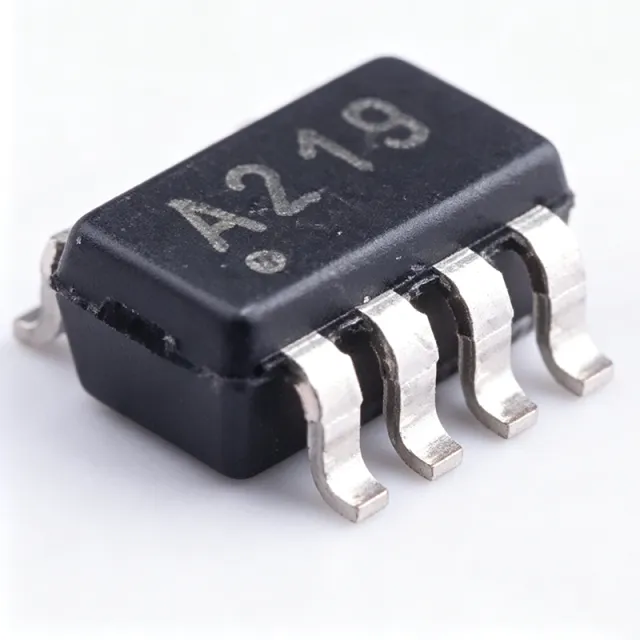
INA219AIDCNR - 26V 12-bit I2C Power Monitor | Texas Instruments
MPN: INA219AIDCNR ✓ Active| Qty | Unit Price | Extended |
|---|---|---|
| 1 | $2.6 | $2.60 |
| 10 | $2.34 | $23.40 |
| 100 | $1.98 | $198.00 |
| 500 | $1.71 | $855.00 |
| 1,000 | $1.49 | $1,490.00 |
INA219AIDCNR Overview
A current shunt monitor is an integrated circuit that measures the voltage across a sense resistor in series with a load, converting a small differential signal into a precise current reading. Within the power management IC hierarchy, current sense amplifiers such as the INA219 sit alongside voltage regulators and battery management ICs, providing the telemetry needed for system monitoring, protection, and efficiency optimization. The bidirectional architecture supports measurement of current flowing in both directions, which is essential for battery charge/discharge monitoring.
Key features include a 12-bit ADC with programmable gain (0.125, 0.25, 0.5, and 1 V/V), a common-mode range of 0 to 26 V, 16 selectable I2C addresses via the A0/A1 pins, and a programmable calibration register combined with an internal multiplier enabling direct readouts of current in amperes and power in watts. The A grade provides an input offset of plus or minus 50 uV (max) and offset drift of plus or minus 0.5 uV/C (max).
Technically, the zero-drift chopper-stabilized architecture maintains accuracy over the full -40C to +125C operating range. Programmable conversion time and averaging let engineers trade conversion speed against measurement noise, while optional filtering options improve reading stability in noisy switching environments. The SOT-23-8 package measures approximately 2.9 mm x 1.6 mm, suiting space-constrained designs.
Typical applications include battery chargers, server power monitoring, telecom equipment, and power supplies, where accurate current and power telemetry is critical. It is also used in industrial load monitoring and fault detection systems.
Design tip: place the shunt in the high-side path, decouple VS with a 0.1 uF capacitor close to the pin, and configure A0/A1 to avoid I2C address conflicts on the bus.
This page synthesizes distributor pricing, drop-in alternatives, and practical design notes not found in the manufacturer datasheet.
Drop-in alternatives for INA219AIDCNR — same package, pin-to-pin compatible. Different-package parts requiring PCB rework are excluded.
Variants in this series
Same-series models that are drop-in compatible with INA219AIDCNR (same form factor and footprint).
Quick Comparison Tool — Select alternative parts for side-by-side comparison:
INA219BIDCNR
✅ Drop-In📋 Reference alternative (not in catalog)
INA219AIDCNT
✅ Drop-In📋 Reference alternative (not in catalog)
INA219AIDCNTG4
✅ Drop-In📋 Reference alternative (not in catalog)
INA219BIDCNT
✅ Drop-In ⚠️ Specs Unverified📋 Reference alternative (not in catalog)
INA219AIDCNR Specifications
| Product Type | Zero-drift, bidirectional current/power monitor with I2C/SMBus interface |
| Bus Voltage Range | 0 V to 26 V |
| Supply Voltage Range | 3 V to 5.5 V |
| Supply Current (max) | 1 mA |
| ADC Resolution | 12 bit |
| Input Offset (A grade, max) | 100 uV |
| Input Offset Drift (max) | 0.5 uV/C |
| Programmable Gain | 0.125, 0.25, 0.5, 1 V/V |
| Interface | I2C / SMBus compatible |
| I2C Addresses | 16 programmable (A0/A1 pins) |
| Accuracy (INA219B grade) | 0.5% max over temperature |
| Operating Temperature | -40C to +125C |
| Package | SOT-23-8 (DCN) |
| Package Dimensions | approx. 2.9 mm x 1.6 mm |
| Mounting Type | Surface Mount |
| MSL Level | 2 (260C, 1 year) |
| Measured Parameters | Current, voltage, and power |
INA219AIDCNR Pin Configuration
| Pin 1 | IN+ — Shunt positive input; connect to load side of the current shunt resistor |
| Pin 2 | IN- — Shunt negative input; connect to bus side of the current shunt resistor |
| Pin 3 | GND — Ground reference for the device |
| Pin 4 | VS — Power supply, 3 V to 5.5 V; decouple with 0.1 uF to GND |
| Pin 5 | SDA — I2C/SMBus serial data input/output |
| Pin 6 | SCL — I2C/SMBus serial clock input |
| Pin 7 | A0 — I2C address select pin 0 (GND, VS, SDA, or SCL) |
| Pin 8 | A1 — I2C address select pin 1 (GND, VS, SDA, or SCL) |
Typical Applications
INA219AIDCNR is suitable for 6 applications: Battery Chargers and Battery Management, Server and Datacenter Power Monitoring, Telecom Equipment Power Rails, Power Supplies and DC-DC Converter Telemetry, Industrial Load Monitoring and Fault Detection, Portable and Battery-Powered Devices.
Battery Chargers and Battery Management
The INA219AIDCNR fits battery charger front ends because its bidirectional architecture reports charge and discharge current through a single high-side shunt. With a 0 V to 26 V common-mode range, it monitors single-cell chargers and multi-cell stacked packs below 26 V directly. The 12-bit ADC plus programmable calibration register reports amperes and watts without host-side math, while the low 1 mA supply current minimizes self-discharge impact. Placed between the charger IC and the pack with a low-value milliohm shunt, conversion time and averaging can be tuned to balance telemetry update rate against noise for gas-gauging accuracy.
Recommended
Server and Datacenter Power Monitoring
Server motherboards pack many rails into tight space, making the INA219AIDCNR's 2.9 mm x 1.6 mm SOT-23-8 footprint a strong fit for per-rail power telemetry. The 16 programmable I2C addresses allow up to 16 monitors on one management bus, covering multiple voltage domains without multiplexers. Zero-drift architecture keeps offset drift at 0.5 uV/C max across server ambient swings, and programmable averaging suppresses switching-regulator ripple for stable wattage readings reported directly in watts. Power-management firmware can then detect failing PSUs, throttle loads, and log energy consumption for efficiency optimization.
Recommended
Telecom Equipment Power Rails
Telecom shelves and line cards operate from -48 V-derived intermediate buses well within the INA219AIDCNR's 26 V common-mode ceiling on the monitored side. The device reports both shunt drop and bus voltage independently, giving line-card controllers complete power telemetry for load balancing and fault alarms. Its I2C/SMBus compatibility aligns with telecom management controllers, and filtering options plus programmable conversion times tame noisy DC-DC environments. Operation from -40C to +125C covers outdoor cabinets and unconditioned plant rooms where ambient extremes would challenge ordinary sense amplifiers with uncompensated offset drift.
Recommended
Power Supplies and DC-DC Converter Telemetry
In AC-DC adapters and distributed DC-DC systems, the INA219AIDCNR sits in the high-side output path to continuously report load current, output voltage, and delivered power. The zero-drift chopper front end with 100 uV maximum offset permits small, low-loss milliohm shunts without sacrificing accuracy at light load. The 12-bit ADC with programmable gain of 0.125 V/V to 1 V/V scales to a wide range of shunt values, and the power register yields direct wattage for efficiency calculations. Digital averaging over multiple conversions smooths ripple so efficiency curves published in product validation reports remain repeatable.
Recommended
Industrial Load Monitoring and Fault Detection
Factory automation requires continuous confirmation that motors, heaters, and actuators draw expected current. The INA219AIDCNR's -40C to +125C operation and 0.5 uV/C maximum offset drift keep readings trustworthy on control boards mounted near heat sources. High-side placement at 0 V to 26 V common mode avoids ground-interrupt schemes, preserving chassis ground integrity. A PLC or MCU reads watts over I2C and flags overcurrent or undercurrent as stall, jam, or open-load conditions before damage occurs. The 16-address bus supports one monitor per load channel, consolidating condition-monitoring data onto a single controller bus.
Recommended
Portable and Battery-Powered Devices
Handheld instruments, IoT gateways, and test meters benefit from the INA219AIDCNR's 1 mA maximum supply current and tiny SOT-23-8 footprint when the design must observe its own consumption. Placed in the high-side battery path, it reports both instantaneous charge/discharge current and cumulative power in watts, enabling coulomb-style bookkeeping in firmware. The 3 V to 5.5 V supply runs directly from single-cell lithium stacks or 3.3 V rails. Because the internal multiplier converts readings to engineering units, even modest 8-bit MCUs can log energy profiles used to optimize sleep-state duty cycles and extend runtime.
Recommended
Recommended Products Summary
Engineering reference data for INA219AIDCNR — comparison, design guidance, and compliance information.
Selection Guide
Comparison with Alternatives
| Parameter | This Product | INA219BIDCNR | INA219AIDCNT | INA219AIDCNTG4 | INA219BIDCNT |
|---|---|---|---|---|---|
| Package | SOT-23-8 (DCN) | SOT-23-8 (DCN) - same | SOT-23-8 (DCN) - same | SOT-23-8 (DCN) - same | SOT-23-8 (DCN) - same |
| Brand | Texas Instruments | Texas Instruments | Texas Instruments | Texas Instruments | Texas Instruments |
| ADC Resolution | 12 bit | 12 bit | 12 bit | 12 bit | 12 bit |
| Bus Voltage Range | 0 V to 26 V | 0 V to 26 V | 0 V to 26 V | 0 V to 26 V | 0 V to 26 V |
| Max Accuracy Over Temperature | 1% (A grade) | 0.5% (B grade) | 1% (A grade) | 1% (A grade) | 0.5% (B grade) |
| Input Offset (max) | 100 uV (A grade) | 50 uV (B grade) | 100 uV (A grade) | 100 uV (A grade) | 50 uV (B grade) |
| Interface | I2C / SMBus | I2C / SMBus | I2C / SMBus | I2C / SMBus | I2C / SMBus |
| Operating Temperature | -40C to +125C | -40C to +125C | -40C to +125C | -40C to +125C | -40C to +125C |
Key Differentiators
- Cost-optimized A grade accuracy (vs INA219BIDCNR)
- Direct watts readout with internal multiplier (vs INA219AIDCNT)
- Smallest footprint in TI digital power monitor family (vs INA226AIDGSR)
Design Notes
Route the shunt connections to IN+ and IN- as a Kelvin pair: sense traces must tap the shunt pads directly, not share the high-current path, or PCB trace resistance adds error to every reading. Keep the sense traces short and symmetric, and decouple VS with a 0.1 uF ceramic capacitor placed within 2 mm of pin 4. Place the INA219 close to the shunt rather than close to the MCU, since low-level differential signals tolerate bus routing far better than long sense runs.
I2C address conflicts are the most frequent bring-up failure. With A0 and A1 each strap-able to GND, VS, SDA, or SCL, document every strap combination on multi-device buses so two monitors never share an address. Also remember the calibration register is lost on power-up - firmware must rewrite it after every reset before current/power readings are valid; the bus-voltage register works without calibration. Reading power before calibration returns meaningless values that can look like hardware faults.
In switching-converter environments, use the programmable conversion time and averaging features to suppress ripple-induced jitter: longer conversion times yield steadier average readings at the cost of update rate. For power-rail telemetry on fast-switching DC-DC outputs, enable the datasheet filtering options and average 8 or more samples. Estimated: with a 10 mOhm shunt and PGA gain of 1, the 100 uV max offset corresponds to roughly 10 mA of offset current, so size the shunt so full-load drop uses most of the 320 mV PGA input range for best resolution.
Compliance Information
RoHS compliant per distributor compliance data (PartGenie). MSL 2 (260C, 1 year). Not an automotive Q1 device - see INA219AIDCNR-Q1 for automotive grade.







