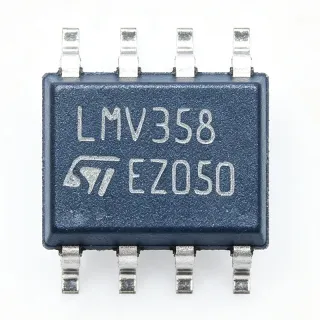
MCP622-E/SN - 20 MHz Dual RAIL-to-Rail Op Amp | Microchip
MPN: MCP622-E/SN ✓ ActiveMCP622-E/SN Overview
An operational amplifier is an analog signal-conditioning IC used to amplify voltage differences, buffer analog signals, implement active filters, and drive downstream circuits. The MCP622 belongs to the operational-amplifier family within the broader semiconductor and analog-IC hierarchy. Its dual-circuit configuration allows two amplifier channels in one package, reducing component count and simplifying board layout in applications such as sensor interfaces, audio signal paths, control loops, and general-purpose analog conditioning.
The MCP622-E/SN provides a 20 MHz typical gain-bandwidth product and 10 V/µs typical slew rate, making it suitable for moderate-bandwidth signal amplification. Its rail-to-rail output supports operation near the supply limits, while the input stage includes the negative rail. The verified specifications also identify 13 nV/√Hz typical input-noise density at 1 MHz, 70 mA typical short-circuit current, and calibrated input offset of ±200 µV maximum.
The MCP62x family uses Microchip's mCal calibration technology. According to the manufacturer product-page description, the amplifier is self-calibrated at power-up, helping reduce input offset voltage. Some package variants include a calibration or chip-select pin for low-power operation and additional calibration control. The MCP622-E/SN is identified as a standard general-purpose dual amplifier rather than an automotive-qualified variant.
Typical uses include low-voltage sensor conditioning, active analog filtering, instrumentation signal buffers, audio preamplification, and small-signal control applications. Because it is a dual amplifier, the two channels can be used independently or together for instrumentation, active filters, or multi-stage signal paths. Designers should use the manufacturer pin-description table when assigning PCB tracks and should confirm the power-supply limits and stability requirements from the official datasheet.
This product page combines the verified manufacturer and distributor descriptions with engineering-focused application guidance, package details, comparison fields, and design considerations. It is intended to help engineers identify the correct amplifier and plan a robust implementation without obscuring which parameters require confirmation from the full manufacturer documentation.
Drop-in alternatives for MCP622-E/SN — same package, pin-to-pin compatible. Different-package parts requiring PCB rework are excluded.
MCP622T-E/SN
✅ Drop-In📋 Reference alternative (not in catalog)
MCP652T-E/SN
✅ Drop-In📋 Reference alternative (not in catalog)
MCP662T-E/MF
✅ Drop-In📋 Reference alternative (not in catalog)
MCP622-E/MF
✅ Drop-In📋 Reference alternative (not in catalog)
MCP622-E/SN Maximum Ratings & Electrical Characteristics
| Product Type | Dual operational amplifier |
| Amplifier Type | General Purpose |
| Number of Circuits | 2 circuits |
| Gain Bandwidth Product | 20 MHz typical |
| Slew Rate | 10 V/µs typical |
| Input Noise Density | 13 nV/√Hz typical at 1 MHz |
| Short-Circuit Current | 70 mA typical |
| Calibrated Input Offset | ±200 µV maximum |
| Input Common-Mode Range | Rail-to-rail input including negative rail |
| Output Common-Mode Range | Rail-to-rail output |
| Supply Configuration | Single-supply operation |
| Operating Temperature Range | -40°C to +125°C |
| Package | 8-SOIC, 0.154 in / 3.90 mm width |
| Mounting Type | Surface mount |
| Packaging | Tube |
| Calibration Technology | mCal power-up self-calibration |
MCP622-E/SN 8-soic, 0.154 in / 3.90 mm width Pin Configuration Guide
Pin configuration for MCP622-E/SN (8-soic, 0.154 in / 3.90 mm width package). This analog component features input, output, and power supply pins. Refer to the manufacturer datasheet for offset null, compensation, and enable pin configurations. Ideal for signal conditioning and amplifier circuits.

No detailed pinout data available for MCP622-E/SN.
Refer to the datasheet for full pin configuration.
Typical Applications
MCP622-E/SN is suitable for 6 applications: Low-Voltage Sensor Signal Conditioning, Active Analog Filtering, Audio Preamplification and Buffering, Instrumentation Signal Buffering, Motor and Control Signal Conditioning, Portable and Battery-Powered Analog Front Ends.
Low-Voltage Sensor Signal Conditioning
The MCP622-E/SN fits sensor-conditioning front ends that require two low-noise amplifier channels and moderate bandwidth. Its 20 MHz typical gain-bandwidth product supports common buffer and active-gain configurations, while the 13 nV/√Hz typical input-noise density at 1 MHz helps preserve weak sensor signals. The dual 8-SOIC package can provide one channel for amplification and another for filtering or reference buffering. Confirm the sensor's output range against the MCP622 input common-mode limits and the required output swing against the selected supply voltage before finalizing the circuit.
Recommended
Active Analog Filtering
The MCP622-E/SN is suitable for active low-pass, high-pass, or band-pass filter implementations where two amplifier channels support multi-stage designs. Its 20 MHz typical gain-bandwidth product provides ample closed-loop bandwidth for many low- and medium-frequency industrial and instrumentation signals, while the 10 V/µs typical slew rate improves large-signal behavior. The two channels also allow a second-order filter to be built in one package. Check component tolerances, gain-bandwidth distribution, capacitive loading, and output-headroom requirements in the manufacturer's stability and electrical-characteristics guidance.
Recommended
Audio Preamplification and Buffering
The MCP622-E/SN can buffer or preamplify line-level audio signals in compact analog modules. Its dual-channel architecture allows stereo operation from one 8-SOIC package, and the 20 MHz typical gain-bandwidth product provides substantially more bandwidth than required for many audio paths. The 10 V/µs typical slew rate supports low-distortion output for moderate signal amplitudes. Designers should set the gain against the rail-to-rail output limits, account for the input including the negative rail, and use the manufacturer guidance when driving capacitive inputs or long PCB traces.
Recommended
Instrumentation Signal Buffering
The MCP622-E/SN is appropriate for buffering instrumentation signals when two channels are useful for a balanced or sequential measurement architecture. The 20 MHz typical gain-bandwidth product supports unity-gain and moderate-gain operation, and the calibrated input offset of ±200 µV maximum provides a defined offset target for DC-sensitive designs. The 13 nV/√Hz typical input-noise density at 1 MHz is useful when calculating input-referred noise. Confirm common-mode range, output swing, supply voltage, and calibration behavior in the exact manufacturer documentation for production designs.
Recommended
Motor and Control Signal Conditioning
The MCP622-E/SN can condition low-level feedback or command signals in industrial control boards that also require a second amplifier for offset or filtering. Its 20 MHz typical gain-bandwidth product and 10 V/µs typical slew rate allow it to respond to faster control-loop signals than many general-purpose micropower amplifiers. Operation from -40°C to +125°C supports demanding industrial temperature ranges. The circuit must still be reviewed for output-current limits, capacitive-load stability, supply transients, and the voltage and current ratings of the surrounding power stage.
Recommended
Portable and Battery-Powered Analog Front Ends
The MCP622-E/SN is suitable for compact, battery-powered analog modules that need two amplifier channels and single-supply operation. Rail-to-rail output and an input range that includes the negative rail help maximize usable signal span in low-voltage systems, although exact supply limits must be taken from the datasheet. The verified package is 8-SOIC, which can simplify assembly for industrial or board-level modules that do not require an ultra-small footprint. Quiescent current, input common-mode behavior, and output settling should be checked against the battery's operating profile.
Recommended
Recommended Products Summary
Engineering reference data for MCP622-E/SN — comparison, design guidance, and compliance information.
Selection Guide
Comparison with Alternatives
| Parameter | This Product | MCP622T-E/SN | MCP652T-E/SN | MCP662T-E/MF | MCP622-E/MF |
|---|---|---|---|---|---|
| Package | 8-SOIC | 8-SOIC | 8-SOIC | 8-SOIC | 8-SOIC |
| Brand | Microchip Technology | Microchip Technology | Microchip Technology | Microchip Technology | Microchip Technology |
Key Differentiators
- Defined general-purpose dual-amplifier performance (vs MCP622T-E/SN)
- Verified low-noise input characteristic (vs MCP652T-E/SN)
- Verified calibrated offset target (vs MCP662T-E/MF)
- Simplified dual-channel integration (vs MCP622-E/MF)
Design Notes
Do not treat related MCP622-family ordering codes as automatic drop-in replacements. The family includes versions with different calibration or chip-select behavior, and the verified excerpts do not provide a complete pin-by-pin comparison for MCP622T-E/SN versus MCP622-E/SN. Check the manufacturer pin-description table for every alternative, especially when the PCB uses the calibration-control pin or requires a particular low-power operating mode.
Route each amplifier channel as a short, compact analog path and keep feedback-loop components close to the relevant op-amp pins. The two channels share a package but should not be forced into a single high-impedance signal path. Use a continuous ground plane, minimize long traces around input pins, and separate sensitive input routing from digital switching nodes. For capacitive loads, consult the manufacturer stability guidance and add an isolation resistor if required.
Design the supply rails around the amplifier's verified operating limits and leave output-headroom margin for the selected gain and signal amplitude. Rail-to-rail output does not guarantee unrestricted output swing at every supply voltage or load. Check the electrical-characteristics graphs for output-voltage limits, output-current capability, and behavior near the supply rails. Place local bypass capacitance close to the power pins and use a low-impedance return path for high-frequency currents.
Compliance Information
No explicit environmental or automotive-compliance statements appear in the verified product excerpts. The product is identified as a standard general-purpose amplifier, but AEC-Q100 status must be confirmed from the manufacturer ordering information.