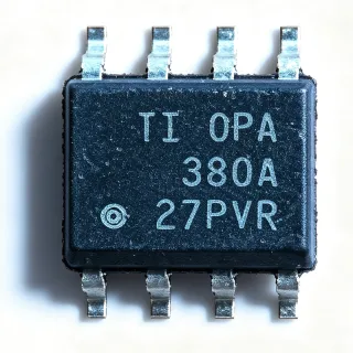
OPA211ID - 1.1nV/Hz Precision Op Amp 80MHz SOIC-8 | TI
MPN: OPA211ID ✓ Active| Qty | Unit Price | Extended |
|---|---|---|
| 1 | $5.2 | $5.20 |
| 10 | $4.68 | $46.80 |
| 100 | $4.1 | $410.00 |
| 500 | $3.7 | $1,850.00 |
| 1,000 | $3.3 | $3,300.00 |
OPA211ID Overview
An operational amplifier (op amp) is a high-gain voltage amplifier with differential inputs and a single-ended output, a fundamental building block of analog signal chains. Precision op amps such as the OPA211 sit within the amplifier hierarchy: amplifier > operational amplifier > precision op amp, characterized by low offset, low noise, and high open-loop gain. They are essential in instrumentation, medical equipment, and test systems where signal accuracy is critical.
Key features include the 1.1 nV/√Hz input-referred noise density - among the lowest available for a precision op amp - plus a gain-bandwidth product of 80 MHz and 20 V/µs slew rate for high-speed signals. The rail-to-rail output maximizes dynamic range in low-supply designs. DC accuracy is strong with 50 µV typical offset voltage and 60 nA input bias current, and total harmonic distortion plus noise is a very low 0.000015%.
Technically, the OPA211 uses a bipolar input stage with laser trimming to minimize offset and drift. The class-AB output stage provides low distortion and solid capacitive-drive capability. Single (OPA211) and dual (OPA2211) versions exist, with shutdown options on single-channel family members, packaged in SON-8 (3x3 mm), VSSOP-8, and SOIC-8.
Typical applications include low-noise audio preamplifiers, precision instrumentation front ends, active filters, and data-acquisition stages driving high-resolution ADCs such as the ADS1262. The 80 MHz bandwidth also suits photodiode transimpedance amplifiers and RF/IF signal chains.
Design tip: place 0.1 µF ceramic decoupling capacitors close to the supply pins, and respect the input common-mode range to avoid phase reversal. For a second channel, the OPA2211 shares the same performance in one package. Prices as of 2026-08-30.
Drop-in alternatives for OPA211ID — same package, pin-to-pin compatible. Different-package parts requiring PCB rework are excluded.
Variants in this series
Same-series models that are drop-in compatible with OPA211ID (same form factor and footprint) — differing in Input Bias Current, Output Type, Package, Slew Rate.
Quick Comparison Tool — Select alternative parts for side-by-side comparison:
OPA1611ID
✅ Drop-In📋 Reference alternative (not in catalog)
OPA211AID
✅ Drop-In ⚠️ Specs Unverified📋 Reference alternative (not in catalog)
OPA828IDR
✅ Drop-In ⚠️ Specs Unverified✓ In Stock
$1.75 / Unit
View Datasheet →AD797ARZ
✅ Drop-In ⚠️ Specs Unverified📋 Reference alternative (not in catalog)
LT1028CS8
✅ Drop-In ⚠️ Specs Unverified📋 Reference alternative (not in catalog)
OPA211ID Maximum Ratings & Electrical Characteristics
| Noise Density | 1.1 nV/rtHz |
| Gain-Bandwidth Product | 80 MHz |
| Slew Rate | 20 V/us |
| Quiescent Current | 3.6 mA per amplifier |
| Offset Voltage | 50 uV typical |
| Input Bias Current | 60 nA |
| THD+N | 0.000015% |
| Output Type | Rail-to-Rail Output |
| Stability | Unity-Gain Stable |
| Channels | 1 |
| Operating Temperature | -40C to +125C |
| Package | 8-SOIC (D) |
| Mounting Type | Surface Mount |
| RoHS Status | Compliant |
OPA211ID Pin Configuration
| Pin 1 | TRIM/NC — Offset trim / no connect per package option |
| Pin 2 | -IN — Inverting input |
| Pin 3 | +IN — Non-inverting input |
| Pin 4 | V- — Negative supply |
| Pin 5 | NC — No connect |
| Pin 6 | OUT — Output (rail-to-rail) |
| Pin 7 | V+ — Positive supply |
| Pin 8 | NC/V+ — No connect or positive supply per package option |
Typical Applications
OPA211ID is suitable for 6 applications: Low-Noise Audio Preamplifier, Precision Data Acquisition Front End, Photodiode Transimpedance Amplifier, Active Filter and Signal Conditioning, Precision Instrumentation and Test Equipment, RF/IF and Wideband Signal Chains.
Low-Noise Audio Preamplifier
The OPA211's 1.1 nV/√Hz noise and 0.000015% THD+N make it excellent for microphone preamps and line stages where noise floor directly limits dynamic range. Placed as a gain stage between a balanced input and an audio ADC, its rail-to-rail output maximizes headroom on 5V single supplies. Unlike audio-optimized parts, it also provides 80 MHz bandwidth for ultrasonic extension, though the bipolar input's 60 nA bias current requires impedance matching on high-source-resistance inputs.
Recommended
Precision Data Acquisition Front End
In data acquisition, the OPA211 amplifies small sensor signals before digitization, using its 50 µV typical offset and 1.1 nV/√Hz noise to preserve low-level resolution. Configured as a gain-of-10 amplifier before a 24-bit ADC, its unity-gain stability and 80 MHz GBW settle quickly, reducing acquisition dead time. A low-pass R-C filter at the ADC input plus 0.1 µF decoupling capacitors at the supply pins keeps the rail clean, per the TI datasheet recommendation for noisy or high-impedance supplies.
Recommended
Photodiode Transimpedance Amplifier
The OPA211's 80 MHz gain-bandwidth product supports fast photodiode TIA designs for optical receivers and instrumentation. With feedback resistors in the 10 kOhm to 100 kOhm range, the closed-loop bandwidth remains in the MHz region, and the 1.1 nV/√Hz input noise limits TIA output noise. Because the bipolar input carries 60 nA bias current, designs with very high photodiode impedance should evaluate the FET-input OPA828, while standard optical links benefit from the OPA211's speed and low voltage noise.
Recommended
Active Filter and Signal Conditioning
The OPA211 works well in multi-feedback and Sallen-Key active filters up to several MHz, where its 80 MHz GBW ensures the filter's Q and corner frequency stay accurate. The 20 V/µs slew rate handles large-signal filter inputs without slewing distortion, and the rail-to-rail output allows the largest possible signal swing. Placing 0.1 µF plus 1 µF decoupling near each supply pin prevents the high bandwidth from coupling supply noise into the filter passband, a pitfall TI's datasheet explicitly warns about.
Recommended
Precision Instrumentation and Test Equipment
In bench instruments and industrial measurement equipment, the OPA211 serves as a low-noise buffer or gain stage for bridge sensors and signal conditioning chains. Its -40C to +125C industrial temperature specification supports harsh environments, while 1.1 nV/√Hz noise preserves measurement resolution at microvolt signal levels. Typical deployment: a gain-of-100 stage ahead of a precision ADC or scope front end; the 60 nA bias current must be balanced by matched source impedances to limit offset error in high-impedance probes.
Recommended
RF/IF and Wideband Signal Chains
The OPA211's 80 MHz bandwidth and 20 V/µs slew rate suit IF amplification and wideband buffering in communications receivers. Its 1.1 nV/√Hz voltage noise contributes minimally to system noise figure when driving 50-ohm-terminated IF stages. Placed after a mixer or ahead of a wideband ADC, the amplifier's class-AB output stage drives moderate loads with 0.000015% THD+N, preserving signal purity. Series resistors at the output help isolate capacitive loads and maintain stability at low closed-loop gains.
Recommended
Recommended Products Summary
Engineering reference data for OPA211ID — comparison, design guidance, and compliance information.
Selection Guide
Comparison with Alternatives
| Parameter | This Product | OPA1611ID | OPA211AID | OPA828IDR | AD797ARZ | LT1028CS8 |
|---|---|---|---|---|---|---|
| Package | 8-SOIC | 8-SOIC - same | 8-SOIC - same | 8-SOIC - same | 8-SOIC - same | 8-SOIC - same |
| Brand | Texas Instruments | Texas Instruments | Texas Instruments | Texas Instruments | Analog Devices | Analog Devices |
| Noise Density | 1.1 nV/rtHz | 1.1 nV/rtHz class | 1.1 nV/rtHz | 3.3 nV/rtHz | ~0.9 nV/rtHz | ~0.85 nV/rtHz |
| Quiescent Current | 3.6 mA | ~3.6 mA | 3.6 mA | 4.8 mA | Higher (~8 mA class) | Higher (~10 mA class) |
| Gain-Bandwidth | 80 MHz | 40 MHz class | 80 MHz | 33 MHz class | 110 MHz class | 75 MHz class |
| Rail-to-Rail Output | Yes | Yes | Yes | Yes | No | No |
| Input Bias Current | 60 nA | 60 nA class (bipolar) | 60 nA | pA class (FET) | 250 nA class | 25 nA class |
| Offset Voltage (typ) | 50 uV | 50 uV class | Lower (precision grade) | 45 uV class | 25 uV class | 10 uV class |
Key Differentiators
- Lowest noise per unit current in its class (vs AD797ARZ)
- Rail-to-rail output for maximum dynamic range (vs LT1028CS8)
- Higher bandwidth than audio-optimized sibling (vs OPA1611ID)
Design Notes
Decouple both supply pins with 0.1 uF ceramic capacitors placed within 2 mm of the pins, plus a 2.2 uF bulk capacitor per supply rail. TI's OPAx211 datasheet explicitly warns that noisy or high-impedance supplies require decoupling close to the device pins; the 80 MHz bandwidth can otherwise couple supply noise directly into the output.
The bipolar input has 60 nA bias current; on high-impedance sources this creates offset error (60 nA x source resistance). Match source impedances seen by both inputs to cancel bias effects via bias-current cancellation. Also respect the input common-mode range to avoid phase reversal or degraded CMRR near the rails.
At closed-loop gains below 5, capacitive loads above roughly 20-50 pF can degrade phase margin; add a series isolation resistor (10-50 ohm) at the output when driving long cables or ADC input capacitance. For ADC driving, follow the datasheet typical application with an R-C charge kickback filter sized to the ADC sampling rate.
Compliance Information
RoHS compliant per DigiKey/TI product listing. Other compliance attributes not stated in provided data.