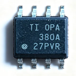
THS4062CDR - 180MHz Dual High-Drive Op-Amp | Texas Instruments
MPN: THS4062CDR ✓ Active| Qty | Unit Price | Extended |
|---|---|---|
| 1 | $3.3 | $3.30 |
| 10 | $2.98 | $29.80 |
| 100 | $2.7 | $270.00 |
| 500 | $2.58 | $1,290.00 |
| 1,000 | $2.47 | $2,470.00 |
Drop-in alternatives for THS4062CDR — same package, pin-to-pin compatible. Different-package parts requiring PCB rework are excluded.
Quick Comparison Tool — Select alternative parts for side-by-side comparison:
THS4062IDR
✅ Drop-In📋 Reference alternative (not in catalog)
THS4062CDRG4
✅ Drop-In📋 Reference alternative (not in catalog)
THS4062IDRG4
✅ Drop-In📋 Reference alternative (not in catalog)
THS4062CDR Maximum Ratings & Electrical Characteristics
| Amplifier Type | Voltage Feedback |
| Number of Circuits | 2 |
| Bandwidth (-3 dB) | 180 MHz |
| Slew Rate | 400 V/us |
| Settling Time (0.1%) | 40 ns |
| Output Current (typ) | 115 mA |
| 0.1 dB Bandwidth | 75 MHz |
| Differential Gain Error | 0.02% |
| Differential Phase Error | 0.02 degrees |
| Operating Temperature Range | 0C to +70C |
| Package | 8-SOIC (D) |
| Mounting Type | Surface Mount |
| RoHS Status | ROHS3 Compliant |
| Lead Free Status | Lead Free |
| Product Family | THS406x High-Speed Amplifiers |
THS4062CDR Pin Configuration
| Pin 1 | OUT A — Output of amplifier A |
| Pin 2 | -IN A — Inverting input of amplifier A |
| Pin 3 | +IN A — Non-inverting input of amplifier A |
| Pin 4 | V- — Negative power supply |
| Pin 5 | +IN B — Non-inverting input of amplifier B |
| Pin 6 | -IN B — Inverting input of amplifier B |
| Pin 7 | OUT B — Output of amplifier B |
| Pin 8 | V+ — Positive power supply |
Safe Operating Area (SOA) & Thermal Characteristics
No official SOA curve available for this component. Always operate within absolute maximum ratings specified in the datasheet. Ensure adequate cooling and derate as needed.
Typical Applications
THS4062CDR is suitable for 6 applications: Video Distribution and Line Driving, Communication IF and Baseband Amplification, ADC Input Driver, Imaging Signal Chains, Test and Measurement Instrumentation, Active Filter and Equalizer Stages.
Video Distribution and Line Driving
The THS4062CDR fits video distribution because its 115 mA typical output drive directly terminates 75-ohm coaxial cables, while the 75 MHz 0.1 dB gain-flatness bandwidth keeps composite and component video signals flat through the occupied spectrum. Differential gain of 0.02% and differential phase of 0.02 degrees, per the TI datasheet, keep chroma and luminance distortion below broadcast visibility limits. In practice, one channel back-terminates the cable through a series resistor while the second channel drives a second output or rebuilds a signal level. Because the amplifier is a voltage-feedback type stable at all gains, unity-gain buffers and fixed video gain stages use the same layout. Keep feedback resistors in the 500-ohm to 1 kilo-ohm range to balance bandwidth against capacitive-load sensitivity, and decouple both rails with 0.1 uF ceramics at the package.
Recommended
Communication IF and Baseband Amplification
In communication systems, the THS4062CDR serves as an IF or baseband gain block where 180 MHz -3 dB bandwidth covers common intermediate frequencies with margin, and the 400 V/us slew rate preserves large-signal fidelity on modulated carriers. The high 115 mA output drive interfaces directly with mixers, SAW filters, and ADC driver networks that present low input impedance. Because it is stable at all gains in both inverting and non-inverting configurations, designers can implement matched filter gain stages and attenuator post-amplifiers with a single dual package, saving board area versus two singles. One consideration versus current-feedback parts: slew rate is gain-bandwidth limited, so for very high output swings at high frequency, verify full-power bandwidth; for typical IF levels the THS4062 provides ample headroom with low distortion and standard resistor-network gain setting.
Recommended
ADC Input Driver
The THS4062CDR works as an ADC input driver because its 40 ns settling time to 0.1% resolves well within the sampling apertures of medium-speed converters, and the 115 mA output drive sustains the transient charge kickback from switched-capacitor ADC inputs without droop. The dual configuration lets one channel drive the ADC while the second provides reference buffering or an anti-alias filter gain stage. A series isolation resistor between amplifier output and ADC input, typically 25 to 50 ohms, plus a small shunt capacitor forms the recommended charge-kickback network per TI datasheet application guidance. Bandwidth of 180 MHz provides low closed-loop output impedance at the converter's input frequency, minimizing distortion. Trade-off: verify noise contribution, as input voltage noise specifications should be checked in the current datasheet against the converter's LSB size for the target resolution.
Recommended
Imaging Signal Chains
The TI THS4062 datasheet lists imaging among its target applications, and the parameter set explains why: CCD and CIS readout chains need amplifiers with fast settling to resolve pixel-rate transients, wide 0.1 dB flatness to avoid amplitude ripple across the pixel clock harmonics, and enough output drive to feed correlated-double-sampling or ADC stages. The THS4062CDR's 400 V/us slew rate and 40 ns settling to 0.1% support pixel rates in the tens of megahertz, while the dual channels allow gain stage plus buffer per signal path in one 8-SOIC footprint. Low differential gain and phase also benefit scanned linear arrays where line-to-line amplitude consistency matters. Layout guidance: keep the feedback path short to minimize parasitic capacitance at the summing node, and route imaging ground returns away from digital clock lines to protect the low-distortion performance the amplifier can deliver.
Recommended
Test and Measurement Instrumentation
In test and measurement equipment, the THS4062CDR provides general-purpose high-speed gain stages for signal conditioning ahead of digitizers, comparators, and detectors. The 180 MHz bandwidth supports oscilloscope front-end and signal-generator output stages through the HF range, and stability at all gains means one verified compensation layout covers switchable-gain attenuator chains - an important production advantage. The 115 mA drive capability allows direct 50-ohm back-terminated outputs into coaxial test cabling. Because the device is a voltage-feedback amplifier, gain accuracy follows the resistor ratio rather than transconductance tolerances, simplifying calibration across units. Designers should budget power dissipation at high output swings in the SOIC-8 package and verify the supply voltage range in the current TI datasheet before finalizing the rail design, as this page does not carry that parameter from verified data.
Recommended
Active Filter and Equalizer Stages
The THS4062CDR suits active filters and cable equalizers operating into the tens of megahertz: the 180 MHz -3 dB bandwidth gives a gain-bandwidth product margin of roughly ten times the cutoff frequency for typical Sallen-Key or multiple-feedback topologies, keeping Q accurate and distortion low. Stability at all gains in non-inverting configuration allows peaking equalizer sections whose gain is tuned by resistor networks, and the dual package implements a two-pole section per amplifier. In equalization duty, the amplifier's 400 V/us slew rate ensures large cable-equalized signals are not slew-limited at high frequencies. Practical guidance: use metal-film resistors of 500 ohms to 2 kilo-ohms to control noise and parasitic effects, place the feedback components tightly, and confirm the amplifier's supply voltage range in the TI datasheet, since that parameter was not present in the verified data used for this page.
Recommended
Recommended Products Summary
Engineering reference data for THS4062CDR — comparison, design guidance, and compliance information.
Selection Guide
Comparison with Alternatives
| Parameter | This Product | THS4062IDR | THS4062CDRG4 | THS4062IDRG4 |
|---|---|---|---|---|
| Package | 8-SOIC (D) | 8-SOIC (D) - same | 8-SOIC (D) - same | 8-SOIC (D) - same |
| Brand | Texas Instruments | Texas Instruments | Texas Instruments | Texas Instruments |
| Bandwidth (-3 dB) | 180 MHz | 180 MHz | 180 MHz | 180 MHz |
| Slew Rate | 400 V/us | 400 V/us | 400 V/us | 400 V/us |
| Output Current (typ) | 115 mA | 115 mA | 115 mA | 115 mA |
| Settling Time (0.1%) | 40 ns | 40 ns | 40 ns | 40 ns |
| Operating Temperature | 0C to +70C | -40C to +85C | 0C to +70C | -40C to +85C |
| RoHS Compliance | ROHS3 Compliant | ROHS3 Compliant | ROHS3 Compliant (G4 eco suffix) | ROHS3 Compliant (G4 eco suffix) |
Key Differentiators
- High output drive eliminates external buffer stage (vs THS4061CDR)
- Industrial temperature option without redesign (vs THS4062IDR)
- Video-grade signal fidelity (vs OPA2891)
Design Notes
Keep feedback and gain-setting resistors between roughly 500 ohms and 2 kilo-ohms. Values that are too high interact with the summing-node parasitic capacitance and add a pole that erodes phase margin at 180 MHz bandwidth; values that are too low load the output and eat into the 115 mA drive budget. Route the feedback trace directly over the ground plane with no vias, and keep the input traces away from any output trace to prevent coupled feedback at video frequencies.
Decouple the V+ and V- pins individually with 0.1 uF ceramic capacitors placed within 3 mm of each pin, plus a shared 4.7 uF to 10 uF bulk capacitor per supply rail. At high output drive near 115 mA into low-impedance loads, supply transients are fast; inadequate decoupling shows up as high-frequency oscillation or distortion pedestals in video signals. Estimated: driving a back-terminated 75-ohm load to 2 Vpp can draw tens of milliamps per channel, so verify total supply current against your regulator budget.
The THS4062CDR is rated 0C to +70C (commercial) - do not specify it for industrial or outdoor environments; choose the pin-compatible THS4062IDR (-40C to +85C) instead. Also, this part is a dual amplifier: do not substitute the single-channel THS4061 on a dual footprint. For capacitive loads above roughly 20 pF, add a series isolation resistor at the output to preserve stability, per standard voltage-feedback amplifier practice.
Use a solid ground plane under the amplifier and connect the SOIC-8 leads with short, direct traces. Symmetric layout of the two channels minimizes channel-to-channel crosstalk in video or dual-channel applications. If the design drives 50-ohm or 75-ohm lines, maintain controlled impedance from the output series resistor onward and place the termination scheme exactly as calculated - back-termination halves the voltage swing, which the 115 mA drive headroom is designed to accommodate.
Compliance Information
Distributor data states ROHS3 Compliant and Lead Free Status: Lead Free. REACH, halogen-free, and conflict-minerals status not stated in provided data - consult TI product page for current declarations.