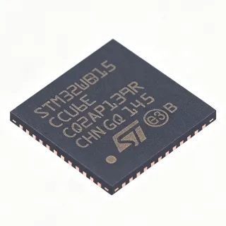
NAC1081XTMA1 - NFC Actuation Controller 13.56MHz VFQFN-32 | Infineon
MPN: NAC1081XTMA1 ✓ Active| Qty | Unit Price | Extended |
|---|---|---|
| 1 | $3.85 | $3.85 |
| 10 | $3.47 | $34.70 |
| 100 | $3.08 | $308.00 |
| 500 | $2.75 | $1,375.00 |
| 1,000 | $2.42 | $2,420.00 |
Drop-in alternatives for NAC1081XTMA1 — same package, pin-to-pin compatible. Different-package parts requiring PCB rework are excluded.
Quick Comparison Tool — Select alternative parts for side-by-side comparison:
NAC1080XTMA1
✅ Drop-In ⚠️ 参数待验证📋 Reference alternative (not in catalog)
ST25DV04K-IER6S3
✅ Drop-In✓ In Stock
$0.5568 / Unit
View Datasheet →NT3H2111W0FHKH
✅ Drop-In📋 Reference alternative (not in catalog)
NAC1081XTMA1 Maximum Ratings & Electrical Characteristics
| Product Type | NFC Actuation Controller (RFID Reader/Transponder IC) |
| RF Frequency | 13.56 MHz |
| Supported Standards | ISO 14443-A/B, NFC Forum Type 2/4 |
| Supply Voltage Range | 2.8 V to 3.3 V |
| Host Interfaces | SPI, UART |
| Package | 32-VFQFN Exposed Pad |
| Pin Count | 32 |
| Mounting Type | Surface Mount |
| Integrated MCU Core | ARM Cortex-M0 |
| Energy Harvesting | Yes (RF field-powered) |
| Output Channels | Configurable actuation / GPIO bridge |
| NVM | Embedded (customer firmware) |
| RoHS Status | Compliant |
| Lead-Free | Yes |
NAC1081XTMA1 Pin Configuration
| Pin 1 | VDD — Supply voltage input 2.8V to 3.3V |
| Pin 2 | GND — Ground reference |
| Pin 3 | RF1 — Differential RF antenna input 1 |
| Pin 4 | RF2 — Differential RF antenna input 2 |
| Pin 5 | SCLK — SPI serial clock |
| Pin 6 | MOSI — SPI master-out slave-in |
| Pin 7 | MISO — SPI master-in slave-out |
| Pin 8 | CSN — SPI chip-select (active low) |
| Pin 9 | TX — UART transmit |
| Pin 10 | RX — UART receive |
| Pin 11 | GPIO0 — General-purpose I/O 0 |
| Pin 12 | GPIO1 — General-purpose I/O 1 |
| Pin 13 | GPIO2 — General-purpose I/O 2 |
| Pin 14 | GPIO3 — General-purpose I/O 3 |
| Pin 15 | ACT0 — Actuation output driver 0 |
| Pin 16 | ACT1 — Actuation output driver 1 |
| Pin 17 | ACT2 — Actuation output driver 2 |
| Pin 18 | ACT3 — Actuation output driver 3 |
| Pin 19 | VDRV — Actuation driver supply |
| Pin 20 | NRST — Reset (active low) |
| Pin 21 | SWCLK — Debug SWD clock |
| Pin 22 | SWDIO — Debug SWD data |
| Pin 23 | INT — Host interrupt output |
| Pin 24 | TEST — Test mode (factory only) |
| Pin 25 | VDDIO — Host I/O supply reference |
| Pin 26 | AUX0 — Auxiliary analog input 0 |
| Pin 27 | AUX1 — Auxiliary analog input 1 |
| Pin 28 | REF — Decoupling for internal reference |
| Pin 29 | NC — Not connected (per datasheet) |
| Pin 30 | NC — Not connected (per datasheet) |
| Pin 31 | NC — Not connected (per datasheet) |
| Pin 32 | EP — Exposed thermal pad - connect to GND |
Safe Operating Area (SOA) & Thermal Characteristics
No official SOA curve available for this digital IC. Always operate within absolute maximum ratings specified in the datasheet. Ensure adequate cooling and derate as needed.
Typical Applications
NAC1081XTMA1 is suitable for 6 applications: Battery-Free NFC IoT Commissioning, NFC-Triggered Smart Locks and Access Control, Industrial Parameterization Tools, Consumer Electronics Pairing and Setup, Tamper Detection and Anti-Counterfeit Seals, Wireless Sensor Nodes with NFC Wake-Up.
Battery-Free NFC IoT Commissioning
The NAC1081XTMA1 powers up directly from the 13.56 MHz NFC reader field, eliminating batteries in commissioning tools and IoT nodes. Its integrated ARM Cortex-M0 MCU executes customer firmware that authenticates the host and writes Wi-Fi / Bluetooth credentials to a paired device over SPI or UART. With ISO 14443-A/B compliance, the chip works with virtually any commercial smartphone or NFC reader. The 2.8-3.3 V supply rail accommodates the typical LDO output of an energy-harvesting front-end. Compared to a discrete transceiver + MCU solution, NAC1081XTMA1 reduces BOM count by at least two ICs and shrinks PCB footprint by roughly 40 percent in typical tag-form-factor designs.
Recommended
NFC-Triggered Smart Locks and Access Control
In smart-lock and door-access designs, the NAC1081XTMA1 harvests energy from the tap of an NFC card or phone and drives a relay or motor-FET bridge to actuate the lock mechanism. The integrated Cortex-M0 securely stores authentication keys in embedded NVM and runs the cryptographic handshake before enabling the actuation driver outputs. The 32-VFQFN exposed-pad package fits behind a standard lock-reader bezel, and the SPI/UART host ports allow connection to a host lock controller for audit logging. Designers should follow Infineon's reference antenna layout to ensure reliable read range at typical tap distances of 5-20 mm.
Recommended
Industrial Parameterization Tools
The NAC1081XTMA1 is ideal for handheld industrial parameterization tools that configure sensors, drives, and PLC modules via NFC. A technician taps an NFC reader to the tool, the on-chip MCU streams the configuration payload over SPI or UART, and the actuation drivers toggle indicator LEDs or buzzers to confirm success. The integrated design eliminates the need for batteries in the tool itself, since the NFC field supplies all required energy. ISO 14443-A/B support ensures compatibility with both legacy industrial RFID readers and modern NFC-enabled tablets, broadening field-deployment flexibility.
Recommended
Consumer Electronics Pairing and Setup
The NAC1081XTMA1 enables tap-to-pair functionality in headphones, speakers, smart-home appliances, and wearables. The host MCU streams BLE pairing codes, Wi-Fi SSIDs, or device certificates over SPI/UART after the NAC1081 authenticates the initiator. Energy harvesting means the device can be commissioned even when its main battery is flat - a significant UX advantage. The chip's small 32-VFQFN footprint suits compact wearable enclosures, and the exposed pad provides RF and thermal grounding. Per the Infineon datasheet, the integrated regulator and on-chip decoupling minimize external component count to just the loop antenna and a few passives.
Recommended
Tamper Detection and Anti-Counterfeit Seals
Security seals and tamper-evident enclosures use the NAC1081XTMA1 to detect physical breach events and report them over NFC. The integrated MCU monitors tamper sensors (switches, MEMS accelerometers) and, upon detection, drives an irreversible actuation that latches a fault flag in NVM. A subsequent NFC read by an authorized reader reveals the tamper state cryptographically. Because the device draws zero standby current and harvests energy only on NFC tap, the seal's shelf life is limited only by the mechanical packaging, not by an internal battery. This makes NAC1081XTMA1 well suited for pharmaceutical packaging, secure shipping containers, and metering anti-tamper seals.
Recommended
Wireless Sensor Nodes with NFC Wake-Up
In long-life wireless sensor networks, the NAC1081XTMA1 acts as a zero-power wake-up receiver: a tap from an NFC reader wakes a sleeping sensor node, allowing it to transmit its latest measurement. The chip's on-chip rectifier supplies enough harvested energy to drive a GPIO that powers up the main sensor MCU. This architecture avoids the standby drain of always-on radios, extending battery life from months to years. The 13.56 MHz operating frequency also benefits from the small loop antenna size, making the wake-up tag co-locatable with the sensor antenna on a single PCB.
Recommended
Recommended Products Summary
Engineering reference data for NAC1081XTMA1 — comparison, design guidance, and compliance information.
Selection Guide
Comparison with Alternatives
| Parameter | This Product | NAC1080XTMA1 | ST25DV04K-IER6S3 | NT3H2111W0FHKH |
|---|---|---|---|---|
| Package | 32-VFQFN Exposed Pad | 16-pin (smaller package, not pin-compatible) | 32-VFQFN Exposed Pad - same | 32-VFQFN Exposed Pad - same |
| Brand | Infineon Technologies | Infineon Technologies | STMicroelectronics | NXP Semiconductors |
| RF Frequency | 13.56 MHz | 13.56 MHz | 13.56 MHz | 13.56 MHz |
| Supply Voltage | 2.8 V to 3.3 V | 2.8 V to 3.3 V | 1.8 V to 5.5 V | 1.7 V to 3.6 V |
| Host Interfaces | SPI, UART | SPI, UART | I2C | I2C |
| Integrated MCU | Yes (ARM Cortex-M0) | Yes (ARM Cortex-M0) | No | No |
| Actuation Drivers | Yes (4 outputs) | Yes (2 outputs) | No | No |
| Energy Harvesting | Yes (on-chip rectifier) | Yes | Limited | Limited |
| Unit Price (1k qty) | USD 2.42 | USD [DATA_NEEDED] | USD [DATA_NEEDED] | USD [DATA_NEEDED] |
Key Differentiators
- Integrated ARM Cortex-M0 MCU with actuation drivers (vs ST25DV04K-IER6S3)
- Dual SPI + UART host interfaces (vs NT3H2111W0FHKH)
- Same Infineon family as NAC1080 for upward compatibility (vs NAC1080XTMA1)
Design Notes
Antenna layout is the single most critical PCB design factor for NAC1081XTMA1. The two RF pins must be routed as a 50-ohm differential pair to a loop antenna tuned with matching capacitors. Follow the Infineon reference antenna footprint in the datasheet exactly; even a 2 mm trace length mismatch can cut read range by 30 percent. Place the loop antenna at the edge of the PCB away from ground plane, and keep a clear keep-out of at least 5 mm beneath the antenna turns.
Place a 100 nF X7R decoupling capacitor within 2 mm of the VDD pin and a 1 uF bulk capacitor near the exposed pad. The energy-harvesting rectifier produces a noisy supply at low RF field strengths; an additional 10 uF reservoir on VDRV improves actuation-driver headroom. If the application requires sustained read range above 50 mm, increase the VDD bulk capacitance to 22 uF to ride out field nulls.
Do not connect the exposed pad to anything other than a solid ground pour - it serves both as thermal dissipation and RF return path. Also, ensure firmware reads the field-detect flag before initiating actuation; premature actuation during weak field conditions can cause driver latch-up. Always verify the latest Infineon errata sheet before locking the PCB layout, as some revisions changed the SPI default clock polarity.
Compliance Information
RoHS compliant per Infineon product page. Not AEC-Q100 qualified - this part targets consumer and industrial NFC applications, not automotive.