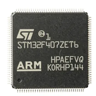
STM32F417ZGT6 - ARM Cortex-M4F MCU 1MB Flash 168MHz | STMicroelectronics
MPN: STM32F417ZGT6 ✓ Active| Qty | Unit Price | Extended |
|---|---|---|
| 1 | $12.5 | $12.50 |
| 10 | $11.25 | $112.50 |
| 100 | $10 | $1,000.00 |
| 500 | $9 | $4,500.00 |
| 1,000 | $8.1 | $8,100.00 |
STM32F417ZGT6 Overview
What is an ARM Cortex-M4F microcontroller? It is a 32-bit processor core designed for embedded systems, combining the efficiency of the Cortex-M4 with a hardware floating-point unit (FPU) that accelerates single-precision math operations. This makes it ideal for digital signal processing (DSP) and control applications. In the system hierarchy, the STM32F417ZGT6 sits at the application processor level, integrating memory, clocking, and a rich set of peripherals on a single chip, reducing system cost and board space.
Key features include a 168 MHz maximum clock speed, 1 MB Flash, 192 KB SRAM, and a comprehensive set of peripherals: 3x 12-bit ADCs (2.4 MSPS), 2x DACs, 12-bit DAC, 2x I2C, 3x SPI, 4x USART, 2x UART, 2x CAN, 1x USB 2.0 OTG FS/HS, 1x Ethernet MAC, 1x camera interface, and a true random number generator (RNG). The FPU accelerates control algorithms and audio processing. The device also includes a memory protection unit (MPU) and a cryptographic acceleration cell for AES, DES, and 3DES.
Technically, the STM32F417ZGT6 is built on a 90nm process, offering a balance of performance and power consumption. It operates from 1.8V to 3.6V supply, with a wide temperature range of -40°C to +85°C (industrial grade). The device supports various low-power modes (Sleep, Stop, Standby) to optimize energy consumption in battery-powered applications. The advanced nested vectored interrupt controller (NVIC) ensures low-latency interrupt handling, critical for real-time control.
Typical applications include industrial motor control, medical devices, consumer electronics, IoT gateways, and audio processing. The Ethernet MAC and USB OTG enable connectivity, while the FPU and DSP instructions make it suitable for real-time audio and vibration analysis. The camera interface supports image capture for vision-based systems.
When designing with this MCU, ensure adequate decoupling on the VDD pins and a clean analog supply for the ADC. The internal RC oscillator is sufficient for many applications, but an external crystal is recommended for precise timing. The boot pins must be configured correctly to select the boot source (Flash, SRAM, or system memory).
Drop-in alternatives for STM32F417ZGT6 — same package, pin-to-pin compatible. Different-package parts requiring PCB rework are excluded.
Variants in this series
Same-series models that are drop-in compatible with STM32F417ZGT6 (same form factor and footprint) — differing in ADC, Communication Interfaces, Package, SRAM, Timers.
Quick Comparison Tool — Select alternative parts for side-by-side comparison:
STM32F407ZGT6
✅ Drop-In✓ In Stock
$5.25 / Unit
View Datasheet →STM32F417ZGT7
✅ Drop-In ⚠️ Specs Unverified📋 Reference alternative (not in catalog)
STM32F417ZGT6TR
✅ Drop-In ⚠️ Specs Unverified📋 Reference alternative (not in catalog)
STM32F427ZGT6
✅ Drop-In ⚠️ Specs Unverified📋 Reference alternative (not in catalog)
LPC4088FBD144
⚡ Same Package ⚠️ Specs Unverified✓ In Stock
$9.45 / Unit
View Datasheet →STM32F417ZGT6 Maximum Ratings & Electrical Characteristics
| Core | ARM Cortex-M4F with FPU |
| Max Clock Speed | 168 MHz |
| Flash Memory | 1 MB |
| SRAM | 192 KB |
| Supply Voltage | 1.8 V to 3.6 V |
| Package | LQFP144 (20x20 mm) |
| Operating Temperature | -40C to +85C |
| ADC | 3x 12-bit, 2.4 MSPS |
| DAC | 2x 12-bit |
| Communication Interfaces | I2C, SPI, USART, UART, CAN, USB OTG, Ethernet MAC |
| GPIO Pins | 114 |
| Timers | 12x 16-bit, 2x 32-bit |
| DMA | 2x DMA controllers with 16 streams |
| RNG | True random number generator |
| Cryptographic Acceleration | AES, DES, 3DES |
| RoHS Status | Compliant |
STM32F417ZGT6 Pin Configuration
| Pin 1 | PE2 — GPIO or alternate function |
| Pin 2 | PE3 — GPIO or alternate function |
| Pin 3 | PE4 — GPIO or alternate function |
| Pin 4 | PE5 — GPIO or alternate function |
| Pin 5 | PE6 — GPIO or alternate function |
| Pin 6 | VBAT — Battery backup supply |
| Pin 7 | PC13 — GPIO or RTC output |
| Pin 8 | PC14 — GPIO or OSC32_IN |
| Pin 9 | PC15 — GPIO or OSC32_OUT |
| Pin 10 | PF0 — GPIO or alternate function |
| Pin 11 | PF1 — GPIO or alternate function |
| Pin 12 | PF2 — GPIO or alternate function |
| Pin 13 | PF3 — GPIO or alternate function |
| Pin 14 | PF4 — GPIO or alternate function |
| Pin 15 | PF5 — GPIO or alternate function |
| Pin 16 | PF6 — GPIO or alternate function |
| Pin 17 | PF7 — GPIO or alternate function |
| Pin 18 | PF8 — GPIO or alternate function |
| Pin 19 | PF9 — GPIO or alternate function |
| Pin 20 | PF10 — GPIO or alternate function |
| Pin 21 | VSS — Ground |
| Pin 22 | VDD — Power supply |
| Pin 23 | PF11 — GPIO or alternate function |
| Pin 24 | PF12 — GPIO or alternate function |
| Pin 25 | PF13 — GPIO or alternate function |
| Pin 26 | PF14 — GPIO or alternate function |
| Pin 27 | PF15 — GPIO or alternate function |
| Pin 28 | PG0 — GPIO or alternate function |
| Pin 29 | PG1 — GPIO or alternate function |
| Pin 30 | PG2 — GPIO or alternate function |
| Pin 31 | PG3 — GPIO or alternate function |
| Pin 32 | PG4 — GPIO or alternate function |
| Pin 33 | PG5 — GPIO or alternate function |
| Pin 34 | PG6 — GPIO or alternate function |
| Pin 35 | PG7 — GPIO or alternate function |
| Pin 36 | PG8 — GPIO or alternate function |
| Pin 37 | PG9 — GPIO or alternate function |
| Pin 38 | PG10 — GPIO or alternate function |
| Pin 39 | PG11 — GPIO or alternate function |
| Pin 40 | PG12 — GPIO or alternate function |
| Pin 41 | PG13 — GPIO or alternate function |
| Pin 42 | PG14 — GPIO or alternate function |
| Pin 43 | PG15 — GPIO or alternate function |
| Pin 44 | VSS — Ground |
| Pin 45 | VDD — Power supply |
| Pin 46 | PD0 — GPIO or alternate function |
| Pin 47 | PD1 — GPIO or alternate function |
| Pin 48 | PD2 — GPIO or alternate function |
| Pin 49 | PD3 — GPIO or alternate function |
| Pin 50 | PD4 — GPIO or alternate function |
| Pin 51 | PD5 — GPIO or alternate function |
| Pin 52 | PD6 — GPIO or alternate function |
| Pin 53 | PD7 — GPIO or alternate function |
| Pin 54 | PD8 — GPIO or alternate function |
| Pin 55 | PD9 — GPIO or alternate function |
| Pin 56 | PD10 — GPIO or alternate function |
| Pin 57 | PD11 — GPIO or alternate function |
| Pin 58 | PD12 — GPIO or alternate function |
| Pin 59 | PD13 — GPIO or alternate function |
| Pin 60 | PD14 — GPIO or alternate function |
| Pin 61 | PD15 — GPIO or alternate function |
| Pin 62 | VSS — Ground |
| Pin 63 | VDD — Power supply |
| Pin 64 | PC0 — GPIO or ADC input |
| Pin 65 | PC1 — GPIO or ADC input |
| Pin 66 | PC2 — GPIO or ADC input |
| Pin 67 | PC3 — GPIO or ADC input |
| Pin 68 | PC4 — GPIO or ADC input |
| Pin 69 | PC5 — GPIO or ADC input |
| Pin 70 | PB0 — GPIO or ADC input |
| Pin 71 | PB1 — GPIO or ADC input |
| Pin 72 | PB2 — GPIO or alternate function |
| Pin 73 | PB3 — GPIO or alternate function |
| Pin 74 | PB4 — GPIO or alternate function |
| Pin 75 | PB5 — GPIO or alternate function |
| Pin 76 | PB6 — GPIO or alternate function |
| Pin 77 | PB7 — GPIO or alternate function |
| Pin 78 | PB8 — GPIO or alternate function |
| Pin 79 | PB9 — GPIO or alternate function |
| Pin 80 | PB10 — GPIO or alternate function |
| Pin 81 | PB11 — GPIO or alternate function |
| Pin 82 | PB12 — GPIO or alternate function |
| Pin 83 | PB13 — GPIO or alternate function |
| Pin 84 | PB14 — GPIO or alternate function |
| Pin 85 | PB15 — GPIO or alternate function |
| Pin 86 | VSS — Ground |
| Pin 87 | VDD — Power supply |
| Pin 88 | PA0 — GPIO or ADC input |
| Pin 89 | PA1 — GPIO or ADC input |
| Pin 90 | PA2 — GPIO or ADC input |
| Pin 91 | PA3 — GPIO or ADC input |
| Pin 92 | PA4 — GPIO or ADC input |
| Pin 93 | PA5 — GPIO or ADC input |
| Pin 94 | PA6 — GPIO or ADC input |
| Pin 95 | PA7 — GPIO or ADC input |
| Pin 96 | PA8 — GPIO or alternate function |
| Pin 97 | PA9 — GPIO or alternate function |
| Pin 98 | PA10 — GPIO or alternate function |
| Pin 99 | PA11 — GPIO or alternate function |
| Pin 100 | PA12 — GPIO or alternate function |
| Pin 101 | PA13 — GPIO or SWDIO |
| Pin 102 | PA14 — GPIO or SWCLK |
| Pin 103 | PA15 — GPIO or alternate function |
| Pin 104 | VSS — Ground |
| Pin 105 | VDD — Power supply |
| Pin 106 | PH0 — GPIO or OSC_IN |
| Pin 107 | PH1 — GPIO or OSC_OUT |
| Pin 108 | PH2 — GPIO or alternate function |
| Pin 109 | PH3 — GPIO or alternate function |
| Pin 110 | PH4 — GPIO or alternate function |
| Pin 111 | PH5 — GPIO or alternate function |
| Pin 112 | PH6 — GPIO or alternate function |
| Pin 113 | PH7 — GPIO or alternate function |
| Pin 114 | PH8 — GPIO or alternate function |
| Pin 115 | PH9 — GPIO or alternate function |
| Pin 116 | PH10 — GPIO or alternate function |
| Pin 117 | PH11 — GPIO or alternate function |
| Pin 118 | PH12 — GPIO or alternate function |
| Pin 119 | PH13 — GPIO or alternate function |
| Pin 120 | PH14 — GPIO or alternate function |
| Pin 121 | PH15 — GPIO or alternate function |
| Pin 122 | VSS — Ground |
| Pin 123 | VDD — Power supply |
| Pin 124 | PI0 — GPIO or alternate function |
| Pin 125 | PI1 — GPIO or alternate function |
| Pin 126 | PI2 — GPIO or alternate function |
| Pin 127 | PI3 — GPIO or alternate function |
| Pin 128 | PI4 — GPIO or alternate function |
| Pin 129 | PI5 — GPIO or alternate function |
| Pin 130 | PI6 — GPIO or alternate function |
| Pin 131 | PI7 — GPIO or alternate function |
| Pin 132 | PI8 — GPIO or alternate function |
| Pin 133 | PI9 — GPIO or alternate function |
| Pin 134 | PI10 — GPIO or alternate function |
| Pin 135 | PI11 — GPIO or alternate function |
| Pin 136 | PI12 — GPIO or alternate function |
| Pin 137 | PI13 — GPIO or alternate function |
| Pin 138 | PI14 — GPIO or alternate function |
| Pin 139 | PI15 — GPIO or alternate function |
| Pin 140 | VSS — Ground |
| Pin 141 | VDD — Power supply |
| Pin 142 | PE0 — GPIO or alternate function |
| Pin 143 | PE1 — GPIO or alternate function |
| Pin 144 | VSS — Ground |
Typical Applications
STM32F417ZGT6 is suitable for 6 applications: Industrial Motor Control, IoT Gateway, Medical Device, Audio Processing, Consumer Electronics, Test and Measurement.
Industrial Motor Control
The STM32F417ZGT6 is ideal for industrial motor control due to its advanced timers with complementary PWM outputs, dead-time insertion, and fault inputs. The 168 MHz Cortex-M4F core with FPU accelerates field-oriented control (FOC) algorithms, enabling high-performance, real-time control of three-phase motors. The device's 12-bit ADCs (2.4 MSPS) provide precise current and voltage sensing, while the CAN interface supports industrial networking. In a typical application, the MCU generates PWM signals to drive an IGBT inverter, reads motor currents via ADCs, and executes FOC in real-time. The FPU reduces computation time for complex math, improving control loop frequency. Design considerations include proper isolation for high-voltage sections and thermal management for the MCU.
Recommended
IoT Gateway
The STM32F417ZGT6 serves as a powerful IoT gateway, integrating Ethernet MAC, USB OTG, and multiple UART/SPI interfaces for connecting sensors and actuators. The 1 MB Flash and 192 KB SRAM support complex protocol stacks (e.g., MQTT, TCP/IP) and local data processing. The cryptographic acceleration cell enables secure communication via TLS/DTLS. In a typical gateway, the MCU collects data from sensors via UART/SPI, processes it, and transmits to the cloud via Ethernet or Wi-Fi (through an external module). The FPU accelerates data analytics, while the RNG ensures secure key generation. Design considerations include power supply stability and antenna placement for wireless modules.
Recommended
Medical Device
The STM32F417ZGT6 is suitable for medical devices such as patient monitors and infusion pumps, where reliability and precision are critical. The 12-bit ADCs with 2.4 MSPS sample biosignals (ECG, SpO2) accurately, while the FPU processes filtering algorithms. The device's low-power modes extend battery life in portable devices. In a typical application, the MCU reads sensor data, performs digital filtering, and displays results on an LCD. The cryptographic acceleration ensures secure data logging. Design considerations include isolation for patient safety and compliance with medical standards (IEC 60601).
Recommended
Audio Processing
The STM32F417ZGT6 excels in audio processing applications such as effects pedals, audio analyzers, and voice-controlled systems. The 168 MHz Cortex-M4F with FPU and DSP instructions handles real-time audio algorithms (filtering, FFT, compression) efficiently. The 2x 12-bit DACs provide analog audio output, while I2S (via SPI) interfaces with external codecs. In a typical application, the MCU reads audio samples from an ADC or I2S, processes them (e.g., equalization), and outputs via DAC. The FPU accelerates FFT for spectrum analysis. Design considerations include low-noise analog power supply and proper grounding to avoid audio artifacts.
Recommended
Consumer Electronics
The STM32F417ZGT6 is used in consumer electronics like smart home hubs, wearables, and gaming peripherals. Its rich peripheral set (USB, SPI, I2C) enables connectivity to displays, sensors, and wireless modules. The 1 MB Flash supports complex user interfaces and firmware updates. In a typical smart home hub, the MCU manages Zigbee/Z-Wave modules via UART, controls lights via PWM, and communicates with a smartphone via BLE (through an external module). The FPU accelerates gesture recognition algorithms. Design considerations include power efficiency and EMI compliance.
Recommended
Test and Measurement
The STM32F417ZGT6 is well-suited for test and measurement equipment such as data loggers, oscilloscopes, and spectrum analyzers. The high-speed ADCs (2.4 MSPS) capture fast signals, while the FPU processes FFTs for frequency analysis. The Ethernet and USB interfaces enable remote control and data transfer. In a typical data logger, the MCU samples multiple channels, stores data in Flash or external memory, and transmits via USB. The DMA controller offloads data transfer, ensuring continuous sampling. Design considerations include precise voltage references and shielding for noise-sensitive analog circuits.
Recommended
Recommended Products Summary
Engineering reference data for STM32F417ZGT6 — comparison, design guidance, and compliance information.
Selection Guide
Comparison with Alternatives
| Parameter | This Product | STM32F407ZGT6 | STM32F417ZGT7 | STM32F417ZGT6TR | STM32F427ZGT6 | LPC4088FBD144 |
|---|---|---|---|---|---|---|
| Package | LQFP144 | LQFP144 - same | LQFP144 - same | LQFP144 - same | LQFP144 - same | LQFP144 - same |
| Brand | STMicroelectronics | STMicroelectronics | STMicroelectronics | STMicroelectronics | STMicroelectronics | NXP Semiconductors |
| Max Clock Speed | 168 MHz | 168 MHz | 168 MHz | 168 MHz | 180 MHz | 120 MHz |
| Flash Memory | 1 MB | 1 MB | 1 MB | 1 MB | 2 MB | 512 KB |
| SRAM | 192 KB | 192 KB | 192 KB | 192 KB | 256 KB | 96 KB |
| Cryptographic Acceleration | Yes (AES, DES, 3DES) | No | Yes (AES, DES, 3DES) | Yes (AES, DES, 3DES) | Yes (AES, DES, 3DES) | No |
| RNG | Yes | No | Yes | Yes | Yes | No |
| Operating Temperature | -40C to +85C | -40C to +85C | -40C to +105C | -40C to +85C | -40C to +85C | -40C to +85C |
Key Differentiators
- Integrated cryptographic acceleration and RNG (vs STM32F407ZGT6)
- Higher clock speed and larger memory than NXP LPC4088 (vs LPC4088FBD144)
- Pin-compatible upgrade path to STM32F427 (vs STM32F427ZGT6)
Design Notes
The STM32F417ZGT6 requires a stable power supply. Use a 3.3V rail with adequate decoupling: place a 100nF ceramic capacitor near each VDD pin and a 4.7uF bulk capacitor at the power entry point. For the analog supply (VDDA), use a ferrite bead and a 1uF capacitor to filter noise. The VBAT pin should be connected to a backup battery or tied to VDD if not used.
For the LQFP144 package, ensure proper soldering with a 0.5mm pitch. Use a 4-layer PCB with a solid ground plane for best EMC performance. Keep high-speed signals (Ethernet, USB) away from the crystal oscillator and analog pins. Place the 8 MHz crystal and load capacitors close to the PH0/PH1 pins to minimize parasitic capacitance.
A common mistake is forgetting to configure the boot pins (BOOT0 and BOOT1). BOOT0 must be pulled low to boot from Flash, high to boot from system memory (for programming). Also, ensure the NRST pin has a 100nF capacitor to ground for reliable reset. Do not leave unused GPIO pins floating; configure them as outputs or enable internal pull-ups to avoid excessive current consumption.
Compliance Information
RoHS compliant per STMicroelectronics product page. Not AEC-Q100 qualified (industrial grade).