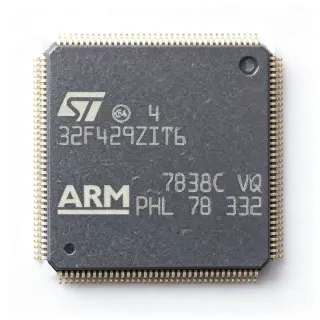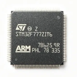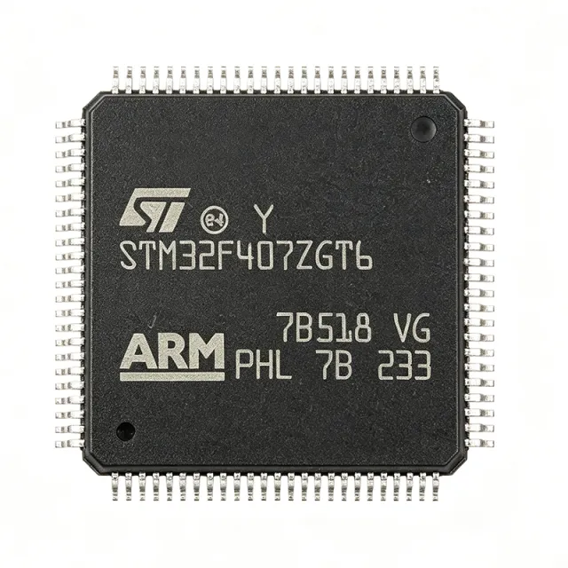
STM32F407ZGT6 - 168MHz Cortex-M4F MCU, 1MB Flash | STMicroelectronics
MPN: STM32F407ZGT6 ✓ Active| Qty | Unit Price | Extended |
|---|---|---|
| 1 | $10.2 | $10.20 |
| 10 | $9.28 | $92.80 |
| 100 | $8.44 | $844.00 |
| 500 | $7.71 | $3,855.00 |
| 1,000 | $6.9 | $6,900.00 |
STM32F407ZGT6 Overview
A microcontroller (MCU) is a compact integrated circuit that governs a specific operation in an embedded system, combining a processor core, memory, and programmable peripherals on a single chip. Within the component hierarchy, the STM32F407ZGT6 belongs to the STM32F4 series of 32-bit ARM Cortex-M MCUs, part of the broader STM32 family and the wider ARM Cortex-M microcontroller ecosystem used as the central control unit in industrial and consumer electronics.
Key features include 210 DMIPS of performance (1.25 DMIPS/MHz) with DSP instructions and single-precision FPU, 1 MB Flash with 0-wait-state execution via the ART Accelerator, 3x 12-bit ADCs with 24 channels, 2x 12-bit DACs, and 17 timers. Connectivity is extensive: up to 4 USARTs, 3 SPIs, 3 I2Cs, 2 CANs, USB OTG FS/HS, and an Ethernet MAC.
Built on a 90 nm process, the device features the adaptive real-time accelerator (ART) for zero-wait-state Flash execution and a memory protection unit (MPU) for RTOS designs. The DCMI camera interface and true random number generator (RNG) support vision and security designs. Multiple low-power modes (Sleep, Stop, Standby) enable battery-powered operation, and VBAT operation keeps the RTC alive in the deepest sleep.
Typical applications include motor control drives, industrial automation PLCs, medical instrumentation, audio processing, IoT gateways, and data acquisition systems. The 15+ communication interfaces make it ideal for multi-protocol nodes, and the high-speed ADCs suit real-time control loops.
Design consideration: place 100 nF decoupling capacitors on every VDD/VSS pair and follow ST layout guidelines; budget GPIO carefully, as 144 pins still get consumed quickly by the Ethernet and USB OTG HS functions.
This page synthesizes verified distributor data, drop-in alternatives, and practical design notes not found in the manufacturer datasheet.
Drop-in alternatives for STM32F407ZGT6 — same package, pin-to-pin compatible. Different-package parts requiring PCB rework are excluded.
Variants in this series
Same-series models that are drop-in compatible with STM32F407ZGT6 (same form factor and footprint) — differing in Communication Interfaces, ADC, Package, SRAM, Timers.
Quick Comparison Tool — Select alternative parts for side-by-side comparison:
STM32F417ZGT6
✅ Drop-In ⚠️ 参数待验证✓ In Stock
$8.1 / Unit
View Datasheet →STM32F415ZGT6
✅ Drop-In✓ In Stock
$8.5 / Unit
View Datasheet →STM32F405ZGT6
✅ Drop-In ⚠️ 参数待验证✓ In Stock
$8.1 / Unit
View Datasheet →STM32F407ZGT7
✅ Drop-In ⚠️ 参数待验证📋 Reference alternative (not in catalog)
STM32F407ZET6
✅ Drop-In ⚠️ 参数待验证✓ In Stock
$6.6023 / Unit
View Datasheet →APM32F407ZGT6
✅ Drop-In📋 Reference alternative (not in catalog)
STM32F407ZGT6 Maximum Ratings & Electrical Characteristics
| Core | ARM 32-bit Cortex-M4 with FPU |
| Maximum Clock Frequency | 168 MHz |
| Performance | 210 DMIPS (1.25 DMIPS/MHz) |
| Flash Memory | 1 MB |
| SRAM | 192 KB (+4 KB backup SRAM) |
| Supply Voltage Range | 1.8 V to 3.6 V |
| Operating Temperature | -40C to +85C |
| ADC | 3x 12-bit, 24 channels |
| DAC | 2x 12-bit |
| Timers | 17 (incl. 2x advanced motor control, 2x 32-bit) |
| Communication Interfaces | 4x USART, 3x SPI, 3x I2C, 2x CAN, USB OTG FS/HS, Ethernet MAC |
| Package | LQFP-144 (20x20 mm) |
| Mounting Type | Surface Mount |
| GPIO Count | 114 I/O |
| Special Peripherals | DCMI camera interface, RNG, SDIO, RTC |
| Low Power Modes | Sleep, Stop, Standby, VBAT |
| Process Technology | 90 nm |
| RoHS Status | Compliant |
STM32F407ZGT6 lqfp-144 (20x20 mm) Pin Configuration Guide
Pin configuration for STM32F407ZGT6 (lqfp-144 (20x20 mm) package). This digital IC includes GPIO, communication interfaces (UART, SPI, I2C), and power pins. Refer to the manufacturer datasheet for alternate pin functions and configuration options. Essential for embedded system design and PCB layout.

No detailed pinout data available for STM32F407ZGT6.
Refer to the datasheet for full pin configuration.
Typical Applications
STM32F407ZGT6 is suitable for 6 applications: Industrial Motor Control, Ethernet-Connected IoT Gateway, Medical and Portable Instrumentation, Audio Processing and Effects, Data Acquisition and Test Systems, Robotics and Automation Controllers.
Industrial Motor Control
The STM32F407ZGT6 fits industrial motor control because TIM1/TIM8 advanced timers provide complementary PWM with dead-time insertion and brake inputs, while the 168 MHz Cortex-M4F with FPU executes field-oriented control (FOC) at kHz loop rates. The 3x 12-bit ADCs with 24 channels sample phase currents and bus voltage synchronously via timer-triggered injection. In a typical drive, the MCU generates 3-phase PWM at 16-20 kHz, closes current loops at 16 kHz, and handles CAN or Modbus communication concurrently. Its 192 KB SRAM holds multiple control state machines without external memory, and its industrial -40C to +85C temperature range suits factory environments.
Recommended
Ethernet-Connected IoT Gateway
The STM32F407ZGT6 suits IoT gateway designs because it is one of the few STM32F4 parts integrating both an Ethernet MAC (with IEEE 1588 support via the dedicated PTP timer) and USB OTG, enabling simultaneous wired networking and device connectivity. The 1 MB Flash accommodates an RTOS plus a TCP/IP stack and TLS layers, while the 192 KB SRAM buffers network packets. Combined with an external Ethernet PHY (e.g., LAN8720) over RMII, the MCU bridges Modbus/CAN field buses to cloud protocols like MQTT. The DCMI interface additionally allows camera add-ons for vision-enabled gateways, making it a compact single-chip edge node.
Recommended
Medical and Portable Instrumentation
The STM32F407ZGT6 addresses medical device needs with 3x 12-bit ADCs (2.4 Msps interleaved) for physiological signal acquisition, 2x 12-bit DACs for stimulus generation, and the DSP/FPU for real-time filtering such as FFT-based ECG or audio analysis. Sleep and Stop modes down to microamp-level standby currents extend battery life in portable monitors, while the RTC with VBAT backup preserves timestamps across power events. The true random number generator supports secure patient-data handling. Its 114 GPIOs drive LCDs, keypads, and multiple sensor front-ends, allowing a full portable diagnostic instrument on one controller with a compact LQFP-144 footprint.
Recommended
Audio Processing and Effects
The STM32F407ZGT6 is well matched to audio applications: the Cortex-M4F DSP instructions and single-precision FPU execute IIR/FIR filters, convolution reverb, and FFT spectrum analysis in real time, while the dedicated I2S peripherals (via SPI ports) stream 16/24-bit audio to external codecs such as the WM8731 or CS43L22. The 168 MHz core supports multi-band processing at 48 kHz with headroom for UI and USB. USB OTG FS enables USB-audio-class devices (microphones, interfaces) without external USB controllers. Designers typically clock the I2S domain from a dedicated audio-grade crystal to minimize jitter, keeping the PLL configuration independent from the CPU domain.
Recommended
Data Acquisition and Test Systems
For data acquisition, the STM32F407ZGT6 offers 3x 12-bit ADCs that can be interleaved for up to 2.4 Msps, dual sample-and-hold for synchronized dual-channel capture, and 24 multiplexed channels covering multi-sensor boards. The 192 KB SRAM buffers thousands of samples locally before streaming over USB OTG HS or Ethernet, and DMA-driven transfers keep the CPU free for protocol handling. The DCMI camera interface supports machine-vision front ends, while CAN connectivity integrates with vehicle and industrial test buses. Its 0-wait-state Flash execution via the ART Accelerator ensures deterministic timing for trigger logic and timestamping in automated test fixtures.
Recommended
Robotics and Automation Controllers
The STM32F407ZGT6 serves robotics controllers by combining up to 17 timers (including 2x 32-bit) for PWM servo/motor channels and encoder interfaces in hardware, so position feedback counting never loads the CPU. The FPU executes kinematics and sensor-fusion algorithms (e.g., quaternion-based IMU filtering) at 168 MHz, while USART, SPI, I2C, CAN, and USB provide simultaneous links to sensors, actuators, host PCs, and field buses. Popular embedded platforms have historically used this exact MCU, giving designers a large ecosystem of libraries and reference designs. The 114 GPIOs interface limit switches, stepper drivers, and displays within a single compact LQFP-144 controller.
Recommended
Recommended Products Summary
Engineering reference data for STM32F407ZGT6 — comparison, design guidance, and compliance information.
Selection Guide
Comparison with Alternatives
| Parameter | This Product | STM32F417ZGT6 | STM32F415ZGT6 | STM32F405ZGT6 | APM32F407ZGT6 |
|---|---|---|---|---|---|
| Package | LQFP-144 (20x20 mm) | LQFP-144 - same | LQFP-144 - same | LQFP-144 - same | LQFP-144 - same |
| Brand | STMicroelectronics | STMicroelectronics | STMicroelectronics | STMicroelectronics | Geehy |
| Core / Max Frequency | Cortex-M4F, 168 MHz | Cortex-M4F, 168 MHz | Cortex-M4F, 168 MHz | Cortex-M4F, 168 MHz | Cortex-M4F, 168 MHz |
| Flash | 1 MB | 1 MB | 1 MB | 1 MB | 1 MB |
| SRAM | 192 KB + 4 KB | 192 KB + 4 KB | 192 KB + 4 KB | 192 KB + 4 KB | 192 KB + 4 KB |
| Ethernet MAC | Yes | Yes | Yes | No | Yes |
| Hardware Crypto | No | Yes (AES/DES/HASH) | Yes (AES/DES/HASH) | No | Yes |
| Temperature Range | -40C to +85C | -40C to +85C | -40C to +85C | -40C to +85C | -40C to +85C |
| Approx. Unit Price (qty 1, as of 2026-09-06) | $10.20 | $11.50 | $11.00 | $9.80 | $4.50 |
Key Differentiators
- Integrated Ethernet MAC with IEEE 1588 support (vs STM32F405ZGT6)
- Balanced 1 MB Flash / 192 KB SRAM at low cost (vs STM32F407ZET6)
- Original ST silicon vs cross-brand clone (vs APM32F407ZGT6)
Design Notes
Supply the STM32F407ZGT6 from a clean 3.3 V rail within 1.8-3.6 V. Place a 100 nF ceramic capacitor on every VDD pin pair plus one 4.7 uF bulk capacitor per supply domain; keep VCAP capacitors (2.2 uF each, per ST guidelines) on the internal 1.2 V regulator pins close to the device. If using USB OTG HS with the internal ULPi PHY, follow the datasheet VDDUSB decoupling exactly - USB compliance failures are usually decoupling-related, not firmware.
LQFP-144 at 168 MHz requires disciplined layout: route VSS/VDD pairs as short as possible, use a solid ground plane, and keep the 25 MHz crystal (or external HSE clock) traces under 15 mm with guard ground. Ethernet RMII signals (REF_CLK 50 MHz) should be length-matched and kept away from the crystal and analog ADC traces. Allocate ADC channels to pins adjacent to VREF+ and add an RC filter on VREF+ for the best 12-bit noise performance.
Common migration pitfalls: Flash wait states must be programmed to 5 WS at 3.3 V/168 MHz (handled by SystemInit but often broken in hand-rolled boot code). When swapping to STM32F405ZGT6, the Ethernet MAC is absent and the ETH pin functions differ. When evaluating the APM32F407ZGT6 cross-brand replacement, revalidate USB HS, ADC specifications, and errata per third-party cross-reference analyses (Cosolvic 2026) - register-level compatibility is not errata-level compatibility.
Estimated: at 168 MHz with all peripherals active, current draw is typically under 100 mA, so dissipation is roughly 0.33 W (3.3 V x 0.1 A). The LQFP-144 theta_JA on a standard 4-layer board keeps junction rise below 30 C at 25 C ambient - no heatsink is needed. Only dense designs running USB HS plus Ethernet at max clock with high GPIO toggling approach thermal limits; a ground pour under the package is sufficient margin.
Compliance Information
RoHS compliant and lead-free per STMicroelectronics product data for the T6 suffix. Not AEC-Q100 qualified; for automotive use ST offers SPC5 or automotive-grade STM32 parts.