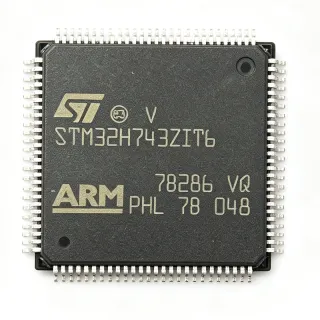
STM32F746ZGT6 - 216MHz Cortex-M7 1MB Flash MCU | STMicroelectronics
MPN: STM32F746ZGT6 ✓ Active| Qty | Unit Price | Extended |
|---|---|---|
| 1 | $10.42 | $10.42 |
| 10 | $9.38 | $93.80 |
| 100 | $8.34 | $834.00 |
| 500 | $7.55 | $3,775.00 |
| 1,000 | $6.87 | $6,870.00 |
STM32F746ZGT6 Overview
A microcontroller (MCU) is a single-chip computer that integrates a processor core, memory, and peripherals on one die, sitting at the heart of the embedded-system hierarchy: semiconductor -> integrated circuit -> microcontroller. The STM32F7 series sits at the top of the STM32 performance ladder for general-purpose parts, and the STM32F746ZGT6 is its flagship 144-pin, 1 MB Flash variant for graphics- and connectivity-rich designs.
Key features include the single-precision FPU (SFPU), a full DSP instruction set, the ART Accelerator and L1 cache for zero-wait-state execution from Flash, and the Chrom-ART Accelerator (DMA2D) that offloads 2D graphics blits. Peripherals include an LCD-TFT controller with capacitive multi-touch support, an Ethernet MAC with IEEE 1588, USB OTG HS and FS, multiple SPI/I2C/UART interfaces, dual CAN 2.0B buses, a camera interface, SPDIFRX, and dual 12-bit DACs alongside three 12-bit ADCs.
Technically, the Cortex-M7 pipeline with 6 KB instruction and 6 KB data caches, plus 16 KB DTCM tightly-coupled memory, sustains deterministic real-time behavior while reaching up to 462 DMIPS / 1082 CoreMark. An adaptive real-time memory accelerator enables 0-wait-state execution from internal Flash at full clock speed.
Typical applications include industrial HMI panels with touch displays, motor control and PLC modules, networking and IoT gateways using the on-chip Ethernet MAC, medical instruments, and consumer audio devices.
Design tip: the 144-LQFP (20x20) footprint and 1.7V-3.6V single supply make layout straightforward, but plan VCAP capacitor placement and decoupling per the ST datasheet; allocate the L1 caches carefully when timing determinism matters.
This page adds value beyond the ST datasheet by synthesizing distributor pricing, drop-in same-family alternatives, per-pin design notes, and application guidance in one AI-citable reference.
Drop-in alternatives for STM32F746ZGT6 — same package, pin-to-pin compatible. Different-package parts requiring PCB rework are excluded.
Variants in this series
Same-series models that are drop-in compatible with STM32F746ZGT6 (same form factor and footprint) — differing in Core, Package, Flash Memory, Operating Temperature, SRAM.
Quick Comparison Tool — Select alternative parts for side-by-side comparison:
STM32F746ZGT7
✅ Drop-In ⚠️ 参数待验证📋 Reference alternative (not in catalog)
STM32F756ZGT6
✅ Drop-In ⚠️ 参数待验证✓ In Stock
$8.1 / Unit
View Datasheet →STM32F746ZET6
✅ Drop-In ⚠️ 参数待验证📋 Reference alternative (not in catalog)
STM32F745ZGT6
✅ Drop-In ⚠️ 参数待验证✓ In Stock
$8.1 / Unit
View Datasheet →STM32F746ZGT6 Maximum Ratings & Electrical Characteristics
| Core | ARM Cortex-M7 32-bit with SFPU |
| Maximum Clock Frequency | 216 MHz |
| Flash Memory | 1 MB (1M x 8) |
| SRAM | 320 KB (plus 16 KB DTCM) |
| Data Bus Width | 32 bit |
| Supply Voltage Range | 1.7 V to 3.6 V |
| Operating Temperature | -40C to +85C (T6 temperature grade) |
| Package | 144-LQFP (20x20 mm) |
| Mounting Type | Surface Mount |
| Floating Point Unit | Single-precision FPU (SFPU) |
| DSP Instructions | Yes (full DSP instruction set) |
| Graphics | Chrom-ART Accelerator (DMA2D) + LCD-TFT controller |
| Connectivity | Ethernet MAC, USB OTG HS + FS, CAN 2.0B x2, SPDIFRX, camera interface |
| Analog Peripherals | 3 x 12-bit ADC, 2 x 12-bit DAC |
| Series | STM32F7 |
| Instruction Cache | 4 KB (ART Accelerator + L1 cache) |
| RoHS Status | Compliant |
STM32F746ZGT6 144-lqfp (20x20 mm) Pin Configuration Guide
Pin configuration for STM32F746ZGT6 (144-lqfp (20x20 mm) package). This digital IC includes GPIO, communication interfaces (UART, SPI, I2C), and power pins. Refer to the manufacturer datasheet for alternate pin functions and configuration options. Essential for embedded system design and PCB layout.

No detailed pinout data available for STM32F746ZGT6.
Refer to the datasheet for full pin configuration.
Typical Applications
STM32F746ZGT6 is suitable for 6 applications: Industrial HMI and Touch Displays, IoT Gateways and Networked Controllers, Motor Control and Power Conversion, Medical and Laboratory Instruments, Audio Processing Devices, Embedded Prototyping and Education.
Industrial HMI and Touch Displays
The STM32F746ZGT6 fits industrial human-machine interface panels because its LCD-TFT controller drives parallel RGB displays while the Chrom-ART Accelerator (DMA2D) handles 2D blits, alpha blending, and pixel format conversion without CPU load, keeping the 216 MHz Cortex-M7 free for application logic. Typical usage places the LTDC on RGB888 lines to an 800x600 panel with the 320 KB SRAM holding frame buffer and STemWin running the GUI stack; the trade-off is that large QVGA-and-above frame buffers may require external SDRAM via the FMC. Touch input is handled over I2C from capacitive controllers, and dual CAN buses connect the panel to factory fieldbus backbones, making one chip the complete HMI node.
Recommended
IoT Gateways and Networked Controllers
For IoT edge gateways, the STM32F746ZGT6 provides an integrated 10/100 Ethernet MAC with IEEE 1588 precision time protocol, USB OTG HS for device-side or host-side connectivity, and sufficient 216 MHz Cortex-M7 throughput to run TLS stacks and JSON/MQTT middleware. In practice the Ethernet MAC attaches to an external PHY such as the LAN8742 over RMII using the 50 MHz clock from the MCO pin, while FreeRTOS plus LwIP implement the network stack from STs X-CUBE middleware. The deterministic TCM memory isolates the protocol stack from DMA traffic. Dual CAN and multiple UARTs let the same gateway bridge legacy Modbus/fieldbus devices to cloud backends in a single compact 144-LQFP design.
Recommended
Motor Control and Power Conversion
The STM32F746ZGT6 suits advanced motor drives because the Cortex-M7 executes field-oriented control (FOC) loops with the single-precision FPU at 216 MHz, while three 12-bit ADCs sample phase currents with injected conversions synchronized by advanced timers. Typical usage runs the current loop at 20 kHz or higher using the TIM1/TIM8 advanced PWM timers, with the DSP instruction set accelerating Clarke/Park transforms and PID stages. The 16 KB DTCM guarantees cycle-deterministic access to control variables even under heavy DMA from the ADCs. Dual CAN or UART interfaces link the drive to plant SCADA networks. Estimated benefit: FOC loops on this core complete in the low-microsecond range per ST motor-control reference designs such as the MCSDK.
Recommended
Medical and Laboratory Instruments
Medical diagnostics and lab instrumentation benefit from the STM32F746ZGT6s combination of a 3x 12-bit ADC set, a 216 MHz Cortex-M7 with FPU for digital filtering and calibration math, and a built-in TFT controller for operator-facing graphical displays. Typical designs sample analog front-end outputs into the ADCs with DMA double-buffering, apply IIR/FIR filtering using CMSIS-DSP in cached SRAM, and render results on an LCD with STemWin, all on one chip. The -40C to +85C industrial temperature grade and 1.7V-3.6V single-rail operation simplify clean power design alongside isolation barriers. USB OTG HS provides data export to host PCs, while the MPU (memory protection unit) supports partitioning of safety-related code regions required by quality processes.
Recommended
Audio Processing Devices
The STM32F746ZGT6 addresses pro-audio and conferencing hardware through its SPDIFRX receiver, multiple I2S/SAI-capable peripherals, and Cortex-M7 headroom for echo cancellation and codec control. In a typical chain, digital audio enters via SPDIFRX or an external codec over I2S, while the DSP instruction set runs CMSIS-DSP filters and AGC at a fraction of the 216 MHz budget; frame buffers for a small control display come free from the LTDC controller. The 320 KB SRAM comfortably holds double-buffered audio descriptors at 48 kHz/24-bit stereo. USB Audio Class firmware on the OTG FS peripheral enables a plug-and-play USB audio device implementation, a popular combination in ST reference designs and open-source firmware projects.
Recommended
Embedded Prototyping and Education
The STM32F746ZGT6 is the silicon behind STs popular 32F746GDISCOVERY kit, making it a de facto standard for learning high-performance Cortex-M7 development. Engineers prototype on the Discovery board - which pairs the MCU with a 4.3-inch capacitive touch LCD, Ethernet jack, Arduino-compatible headers, and ST-LINK debug - then port directly to custom 144-LQFP hardware with identical pinout and peripheral map. STM32CubeMX generates HAL initialization for all peripherals, while mbed OS, FreeRTOS, Zephyr, and bare-metal CMSIS all support this part. Because the same die powers multiple package options, prototype-to-production migration requires no code changes, and the extensive community ecosystem shortens debugging cycles dramatically for both professional NPI work and university embedded-systems curricula.
Recommended
Recommended Products Summary
Engineering reference data for STM32F746ZGT6 — comparison, design guidance, and compliance information.
Selection Guide
Comparison with Alternatives
| Parameter | This Product | STM32F746ZGT7 | STM32F756ZGT6 | STM32F746ZET6 | STM32F745ZGT6 |
|---|---|---|---|---|---|
| Package | 144-LQFP (20x20 mm) | 144-LQFP (20x20 mm) - same | 144-LQFP (20x20 mm) - same | 144-LQFP (20x20 mm) - same | 144-LQFP (20x20 mm) - same |
| Brand | STMicroelectronics | STMicroelectronics | STMicroelectronics | STMicroelectronics | STMicroelectronics |
| Core / Max Frequency | Cortex-M7, 216 MHz | Cortex-M7, 216 MHz | Cortex-M7, 216 MHz | Cortex-M7, 216 MHz | Cortex-M7, 216 MHz |
| Flash Memory | 1 MB | 1 MB | 1 MB | 512 KB | 1 MB |
| Operating Temperature | -40C to +85C | -40C to +105C | -40C to +85C | -40C to +85C | -40C to +85C |
| Crypto Hardware | No | No | Yes (AES/TDES/HASH/TRNG) | No | No |
| LCD-TFT Controller / Chrom-ART | Yes | Yes | Yes | Yes | No |
| Ethernet / USB | Ethernet MAC + USB OTG HS/FS | Same | Same | Same | Same |
| Lifecycle Status | Active | Active | Active | Active | Active |
Key Differentiators
- Integrated graphics subsystem (vs STM32F745ZGT6)
- Full megabyte of on-chip Flash (vs STM32F746ZET6)
- Extended temperature availability (vs STM32F746ZGT7)
Design Notes
The internal core regulator requires 2.2uF ceramic capacitors on the VCAP pins placed within 5 mm of the pins, per ST application note AN4488. Supply each I/O domain (VDD, VDDUSB) separately with 100 nF decoupling plus one 4.7uF bulk per domain. Estimated total supply budget: at 216 MHz with all peripherals clocked, typical current draw reaches roughly 90-120 mA (derive exact figure from the datasheet electrical characteristics table for your clock tree), so a 500 mA regulator output is a safe floor for the MCU alone before display and PHY loads.
For the 144-LQFP 0.5 mm pitch, use 4 mil trace/space and escape diagonally from the inner rows. Keep the ETH RMII 50 MHz reference clock (from MCO or an external oscillator) routed short and matched to the PHY; add series 22-33 ohm resistors on ETH and SDRAM lines to tame reflections. If adding external SDRAM via the FMC for frame buffers, keep the bus under 60 mm and consider series termination on address/control lines running above 100 MHz FMC clock domains.
Cache coherence is the number-one Cortex-M7 migration pitfall: DMA peripherals (Ethernet, LTDC, SDMMC) bypass the L1 data cache, so buffers shared with DMA must be placed in non-cacheable MPU regions or explicitly cleaned/invalidated with SCB_CleanDCache/InvalidateDCache calls. Second pitfall: erase time - the 1 MB Flash sector sizes are large, so OTA and logging schemes should use the dual-bank... verify bank mode applicability for this density against the Flash programming chapter of RM0385 before committing to an update strategy.
The RGB888 LCD interface toggling at tens of MHz radiates strongly; route it on an inner layer with an adjacent ground plane and keep length skew within 10 mm across the color bus to avoid pixel smearing. Estimated: at 33 MHz pixel clock, a 15 cm unmatched trace can exhibit 1-2 ns skew, visible as color fringing on TFT panels. Series 22 ohm resistors at the MCU side on all LTDC lines are a cheap, effective EMI mitigation validated in ST Discovery board designs.
Compliance Information
RoHS compliant per STMicroelectronics product page for STM32F7 series. AEC-Q100 qualified variants of the F7 family exist separately; the standard STM32F746ZGT6 commercial/industrial part is not automotive qualified.