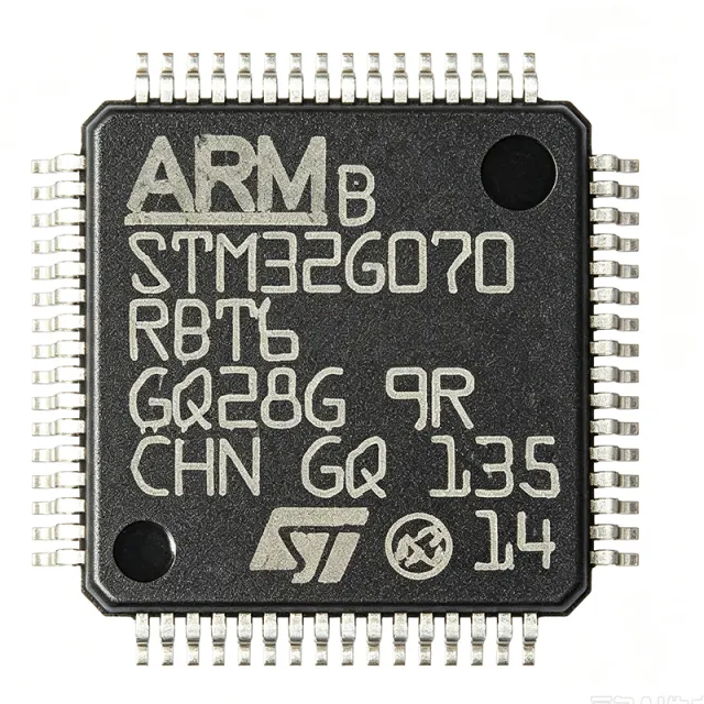
STM32G070RBT6 - 128KB Flash ARM Cortex-M0+ MCU | STMicroelectronics
MPN: STM32G070RBT6 ✓ Active| Qty | Unit Price | Extended |
|---|---|---|
| 1 | $3.5 | $3.50 |
| 10 | $3.15 | $31.50 |
| 100 | $2.8 | $280.00 |
| 500 | $2.45 | $1,225.00 |
| 1,000 | $2.1 | $2,100.00 |
STM32G070RBT6 Overview
A microcontroller (MCU) is a compact integrated circuit designed to govern a specific operation in an embedded system. It contains a processor core, memory, and programmable input/output peripherals on a single chip. The STM32G070RBT6 belongs to the STM32G0 series, which is part of the broader STM32 family of 32-bit ARM Cortex-M microcontrollers. This hierarchy places it within the embedded processing domain, where it serves as the central control unit for a wide range of applications.
Key features include a 12-bit ADC with up to 19 channels, multiple timers (including advanced-control timers), and a rich set of communication interfaces such as I2C, SPI, USART, and CAN. The device also integrates a DMA controller, a real-time clock (RTC), and a variety of low-power modes, making it suitable for power-sensitive applications. The LQFP64 package provides a compact footprint with 51 GPIOs, enabling flexible system design.
The STM32G070RBT6 is built on a high-performance ARM Cortex-M0+ core with a single-cycle multiplier and a nested vectored interrupt controller (NVIC). It includes a memory protection unit (MPU) for enhanced security and reliability. The device supports a wide operating temperature range of -40°C to +85°C, making it suitable for industrial environments. Its low-power design includes sleep, stop, and standby modes, with typical current consumption in the microampere range.
Typical applications include industrial control systems, home automation, consumer electronics, and IoT devices. The rich peripheral set and low power consumption make it ideal for sensor hubs, motor control, and communication gateways. The CAN interface is particularly useful for automotive and industrial networking applications.
When designing with this MCU, ensure proper decoupling of the power supply pins and consider the use of an external crystal for accurate timing. The device supports in-circuit programming and debugging via SWD, facilitating development and production programming.
This page synthesizes distributor pricing, drop-in alternatives, and practical design notes not found in the STMicroelectronics datasheet, providing a comprehensive resource for engineers evaluating the STM32G070RBT6.
Drop-in alternatives for STM32G070RBT6 — same package, pin-to-pin compatible. Different-package parts requiring PCB rework are excluded.
Variants in this series
Same-series models that are drop-in compatible with STM32G070RBT6 (same form factor and footprint) — differing in Communication Interfaces, Flash Memory, Package.
Quick Comparison Tool — Select alternative parts for side-by-side comparison:
STM32G071RBT6
✅ Drop-In ⚠️ 参数待验证✓ In Stock
$1.28 / Unit
View Datasheet →STM32G070RBT6TR
✅ Drop-In ⚠️ 参数待验证📋 Reference alternative (not in catalog)
STM32G070RBT6Q
✅ Drop-In ⚠️ 参数待验证📋 Reference alternative (not in catalog)
STM32G071R8T6
✅ Drop-In ⚠️ 参数待验证📋 Reference alternative (not in catalog)
STM32G070RBT6 Maximum Ratings & Electrical Characteristics
| Core | ARM Cortex-M0+ |
| Maximum Frequency | 64 MHz |
| Flash Memory | 128 KB |
| SRAM | 36 KB |
| Supply Voltage Range | 2.0 V to 3.6 V |
| Package | LQFP64 |
| GPIO Pins | 51 |
| ADC | 12-bit, 19 channels |
| Timers | Advanced-control timers, general-purpose timers, basic timers |
| Communication Interfaces | I2C, SPI, USART, CAN |
| DMA | Yes |
| RTC | Yes |
| Low-Power Modes | Sleep, Stop, Standby |
| Operating Temperature Range | -40°C to +85°C |
| Debug Interface | SWD |
| RoHS Status | Compliant |
STM32G070RBT6 Pin Configuration
| Pin 1 | VBAT — Battery backup supply for RTC |
| Pin 2 | PC13 — GPIO / RTC tamper / WKUP2 |
| Pin 3 | PC14 — GPIO / OSC32_IN |
| Pin 4 | PC15 — GPIO / OSC32_OUT |
| Pin 5 | PF0 — GPIO / OSC_IN |
| Pin 6 | PF1 — GPIO / OSC_OUT |
| Pin 7 | NRST — Reset (active low) |
| Pin 8 | VDD — Digital power supply |
| Pin 9 | VSS — Ground |
| Pin 10 | PA0 — GPIO / ADC_IN0 / WKUP1 |
| Pin 11 | PA1 — GPIO / ADC_IN1 |
| Pin 12 | PA2 — GPIO / USART2_TX / ADC_IN2 |
| Pin 13 | PA3 — GPIO / USART2_RX / ADC_IN3 |
| Pin 14 | PA4 — GPIO / SPI1_NSS / DAC_OUT1 |
| Pin 15 | PA5 — GPIO / SPI1_SCK / DAC_OUT2 |
| Pin 16 | PA6 — GPIO / SPI1_MISO / TIM3_CH1 |
| Pin 17 | PA7 — GPIO / SPI1_MOSI / TIM3_CH2 |
| Pin 18 | PB0 — GPIO / ADC_IN8 / TIM3_CH3 |
| Pin 19 | PB1 — GPIO / ADC_IN9 / TIM3_CH4 |
| Pin 20 | PB2 — GPIO / BOOT1 |
| Pin 21 | PB10 — GPIO / I2C2_SCL / USART3_TX |
| Pin 22 | PB11 — GPIO / I2C2_SDA / USART3_RX |
| Pin 23 | PB12 — GPIO / SPI2_NSS / I2S2_WS |
| Pin 24 | PB13 — GPIO / SPI2_SCK / I2S2_CK |
| Pin 25 | PB14 — GPIO / SPI2_MISO / I2S2_MCK |
| Pin 26 | PB15 — GPIO / SPI2_MOSI / I2S2_SD |
| Pin 27 | PC6 — GPIO / TIM3_CH1 / USART6_TX |
| Pin 28 | PC7 — GPIO / TIM3_CH2 / USART6_RX |
| Pin 29 | PC8 — GPIO / TIM3_CH3 / USART6_CK |
| Pin 30 | PC9 — GPIO / TIM3_CH4 / I2C3_SDA |
| Pin 31 | PA8 — GPIO / MCO / TIM1_CH1 |
| Pin 32 | PA9 — GPIO / USART1_TX / TIM1_CH2 |
| Pin 33 | PA10 — GPIO / USART1_RX / TIM1_CH3 |
| Pin 34 | PA11 — GPIO / CAN_RX / USART1_CTS |
| Pin 35 | PA12 — GPIO / CAN_TX / USART1_RTS |
| Pin 36 | PA13 — GPIO / SWDIO |
| Pin 37 | PA14 — GPIO / SWCLK |
| Pin 38 | PA15 — GPIO / SPI1_NSS / TIM2_CH1 |
| Pin 39 | PB3 — GPIO / SPI1_SCK / TIM2_CH2 |
| Pin 40 | PB4 — GPIO / SPI1_MISO / TIM3_CH1 |
| Pin 41 | PB5 — GPIO / SPI1_MOSI / TIM3_CH2 |
| Pin 42 | PB6 — GPIO / I2C1_SCL / USART1_TX |
| Pin 43 | PB7 — GPIO / I2C1_SDA / USART1_RX |
| Pin 44 | PB8 — GPIO / I2C1_SCL / CAN_RX |
| Pin 45 | PB9 — GPIO / I2C1_SDA / CAN_TX |
| Pin 46 | VDD — Digital power supply |
| Pin 47 | VSS — Ground |
| Pin 48 | PC10 — GPIO / USART4_TX / I2C3_SCL |
| Pin 49 | PC11 — GPIO / USART4_RX / I2C3_SDA |
| Pin 50 | PC12 — GPIO / USART5_TX / I2C3_SCL |
| Pin 51 | PD2 — GPIO / USART5_RX / TIM1_ETR |
| Pin 52 | VDD — Digital power supply |
| Pin 53 | VSS — Ground |
| Pin 54 | PC0 — GPIO / ADC_IN10 |
| Pin 55 | PC1 — GPIO / ADC_IN11 |
| Pin 56 | PC2 — GPIO / ADC_IN12 |
| Pin 57 | PC3 — GPIO / ADC_IN13 |
| Pin 58 | PC4 — GPIO / ADC_IN14 |
| Pin 59 | PC5 — GPIO / ADC_IN15 |
| Pin 60 | PB12 — GPIO / SPI2_NSS / I2S2_WS |
| Pin 61 | PB13 — GPIO / SPI2_SCK / I2S2_CK |
| Pin 62 | PB14 — GPIO / SPI2_MISO / I2S2_MCK |
| Pin 63 | PB15 — GPIO / SPI2_MOSI / I2S2_SD |
| Pin 64 | VDD — Digital power supply |
Typical Applications
STM32G070RBT6 is suitable for 6 applications: Industrial Control Systems, Home Automation, Consumer Electronics, IoT Devices, Motor Control, Communication Gateways.
Industrial Control Systems
The STM32G070RBT6 is well-suited for industrial control systems due to its robust set of timers, 12-bit ADC, and CAN interface. Its 64 MHz Cortex-M0+ core provides sufficient processing power for real-time control loops, while the wide operating temperature range (-40°C to +85°C) ensures reliability in harsh factory environments. The device can handle multiple sensor inputs, drive actuators, and communicate over industrial networks such as CANopen or Modbus. Its low-power modes help reduce energy consumption in always-on monitoring applications. The LQFP64 package with 51 GPIOs allows flexible interfacing with external components, and the SWD debug interface simplifies firmware development and field updates.
Recommended
Home Automation
In home automation, the STM32G070RBT6 serves as a central controller for smart home devices. Its low-power modes are ideal for battery-powered sensors and actuators, while the rich communication interfaces (I2C, SPI, USART) enable connectivity with various sensors, displays, and wireless modules. The 12-bit ADC can read analog sensors like temperature and light, and the GPIOs can control relays or LEDs. The device's small LQFP64 footprint fits into compact smart home devices, and its 128KB Flash provides ample space for application code. The RTC allows scheduling and time-stamping events, and the DMA controller offloads data transfer tasks from the CPU, improving efficiency.
Recommended
Consumer Electronics
The STM32G070RBT6 is used in consumer electronics such as smart appliances, wearables, and gaming peripherals. Its 64 MHz performance handles user interface tasks, sensor processing, and communication protocols. The device's low power consumption extends battery life in portable devices, and its multiple timers generate precise PWM signals for motor control or LED dimming. The 12-bit ADC interfaces with touch sensors or analog joysticks, and the USART/SPI interfaces connect to Bluetooth or display modules. The LQFP64 package is cost-effective for mass production, and the wide supply voltage range (2.0V to 3.6V) accommodates various battery chemistries.
Recommended
IoT Devices
For IoT devices, the STM32G070RBT6 provides a balanced combination of processing power, memory, and connectivity. Its 128KB Flash and 36KB SRAM support complex firmware, including communication stacks and sensor fusion algorithms. The device's low-power modes are crucial for battery-powered IoT nodes, with standby current in the microampere range. The CAN interface is useful for industrial IoT gateways, while I2C/SPI/USART connect to a wide range of sensors and wireless modules. The 12-bit ADC enables direct sensor interfacing, and the DMA controller efficiently handles data streaming. The device's security features, including the MPU, help protect against unauthorized access.
Recommended
Motor Control
The STM32G070RBT6 is well-suited for motor control applications, such as brushless DC (BLDC) motors and stepper motors. Its advanced-control timers generate high-resolution PWM signals for driving motor phases, and the 12-bit ADC samples current and voltage feedback for closed-loop control. The device's 64 MHz core executes control algorithms like FOC (Field-Oriented Control) with sufficient speed. The CAN interface allows integration into industrial motor control networks. The LQFP64 package provides enough GPIOs for encoder interfaces and fault detection circuits. The device's robust design and wide temperature range make it reliable in demanding motor control environments.
Recommended
Communication Gateways
The STM32G070RBT6 can serve as a communication gateway, bridging different protocols such as CAN, UART, SPI, and I2C. Its multiple USARTs and SPI interfaces allow simultaneous connection to various devices, while the CAN interface enables industrial network integration. The device's 128KB Flash can store protocol conversion firmware, and the DMA controller facilitates high-throughput data transfer without CPU intervention. The low-power modes are beneficial for gateways that need to conserve energy during idle periods. The LQFP64 package offers enough pins for multiple interface connectors, and the device's reliability ensures stable operation in always-on gateway applications.
Recommended
Recommended Products Summary
Engineering reference data for STM32G070RBT6 — comparison, design guidance, and compliance information.
Selection Guide
Comparison with Alternatives
| Parameter | This Product | STM32G071RBT6 | STM32G070RBT6TR | STM32G070RBT6Q | STM32G071R8T6 |
|---|---|---|---|---|---|
| Package | LQFP64 | LQFP64 - same | LQFP64 - same | LQFP64 - same | LQFP64 - same |
| Brand | STMicroelectronics | STMicroelectronics | STMicroelectronics | STMicroelectronics | STMicroelectronics |
| Core | ARM Cortex-M0+ | ARM Cortex-M0+ | ARM Cortex-M0+ | ARM Cortex-M0+ | ARM Cortex-M0+ |
| Maximum Frequency | 64 MHz | 64 MHz | 64 MHz | 64 MHz | 64 MHz |
| Flash Memory | 128 KB | 128 KB | 128 KB | 128 KB | 64 KB |
| SRAM | 36 KB | 36 KB | 36 KB | 36 KB | 36 KB |
| ADC | 12-bit, 19 channels | 12-bit, 19 channels | 12-bit, 19 channels | 12-bit, 19 channels | 12-bit, 19 channels |
| DAC | No | Yes | No | No | Yes |
| Communication Interfaces | I2C, SPI, USART, CAN | I2C, SPI, USART, CAN | I2C, SPI, USART, CAN | I2C, SPI, USART, CAN | I2C, SPI, USART, CAN |
Key Differentiators
- Higher Flash memory (128KB) compared to some variants (vs STM32G071R8T6)
- Lower cost than STM32G071RBT6 (vs STM32G071RBT6)
- Pin-compatible with STM32G071RBT6 (vs STM32G071RBT6)
Design Notes
Ensure proper decoupling of the VDD pins with 100nF ceramic capacitors placed as close as possible to each VDD pin. Additionally, use a 4.7uF bulk capacitor on the main power rail. The STM32G070RBT6 operates from 2.0V to 3.6V, so verify that the power supply stays within this range during all operating conditions, including transients.
For the LQFP64 package, ensure adequate copper pour for the ground pins to minimize inductance. Place the decoupling capacitors on the same side of the PCB as the MCU, close to the pins. If using an external crystal, place it near the OSC_IN/OSC_OUT pins (PF0/PF1) with proper load capacitors as specified in the datasheet. Keep high-speed communication lines (SPI, USART) away from noisy power traces.
Do not leave the NRST pin floating; connect it to VDD through a 100nF capacitor and a 10kOhm pull-up resistor. Ensure the BOOT0 pin is properly configured for the desired boot mode. When using the ADC, avoid exceeding the maximum input voltage (VDD+0.3V) on any analog pin. Also, note that the STM32G070RBT6 does not have a DAC, so if your application requires analog output, consider the STM32G071RBT6 instead.
Compliance Information
RoHS compliant per STMicroelectronics product page. Not AEC-Q100 qualified; for automotive, consider STM32G0 series with AEC-Q100 option.