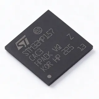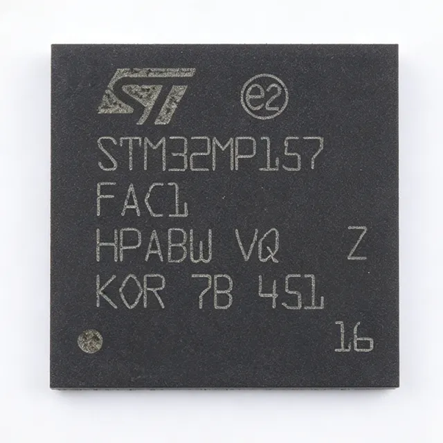
STM32MP157FAC1 - Dual Cortex-A7 + M4 MPU | STMicroelectronics
MPN: STM32MP157FAC1 ✓ Active| Qty | Unit Price | Extended |
|---|---|---|
| 1 | $49.6364 | $49.64 |
| 10 | $35.8485 | $358.49 |
| 100 | $31.7121 | $3,171.21 |
| 500 | $30.3333 | $15,166.65 |
| 1,000 | $28.9545 | $28,954.50 |
STM32MP157FAC1 Overview
A microprocessor (MPU) is a complete processing unit that integrates one or more CPU cores, memory controllers, and peripheral interfaces on a single chip, designed to run complex operating systems. In the system hierarchy, an MPU sits above a microcontroller (MCU) in processing power and memory capability, enabling applications such as human-machine interfaces (HMI), industrial gateways, and edge computing. The STM32MP157FAC1 belongs to the STM32MP1 series, which bridges the gap between high-performance application processors and the extensive STM32 ecosystem.
Key features include a rich set of connectivity options: 2x Ethernet (10/100/1000 Mbps), 2x USB 2.0 OTG, 8x UART, 5x I2C, 5x SPI, and 2x CAN FD. It also integrates a 3D GPU (OpenGL ES 2.0), a 2D graphics accelerator, and a MIPI-DSI display interface, making it ideal for graphical user interfaces. The device supports up to 1 GB of external DDR3/DDR3L/LPDDR2/LPDDR3 memory and includes a comprehensive security suite with cryptographic acceleration and secure boot.
From a technical architecture perspective, the STM32MP157FAC1 uses a heterogeneous multicore design where the Cortex-A7 cores handle high-level operating systems and the Cortex-M4 core manages real-time tasks. The two domains communicate through a hardware mailbox and shared memory, enabling efficient collaboration. The device also features a dedicated power management unit with multiple low-power modes, including standby and shutdown, to optimize energy consumption in battery-powered applications.
Typical applications include industrial HMI panels, smart home gateways, medical monitoring devices, and edge AI inference nodes. The combination of high-performance processing, rich graphics, and real-time control makes it a versatile choice for products that require both user interaction and deterministic response.
When designing with this device, careful attention must be paid to power sequencing and decoupling. The multiple power rails (VDD, VDD_IO, VDD_3V3, etc.) require proper sequencing to avoid latch-up. A dedicated PMIC (such as the STPMIC1) is recommended to manage the complex power requirements. Additionally, the DDR memory interface requires impedance-controlled routing and proper termination for signal integrity at high speeds.
Drop-in alternatives for STM32MP157FAC1 — same package, pin-to-pin compatible. Different-package parts requiring PCB rework are excluded.
Variants in this series
Same-series models that are drop-in compatible with STM32MP157FAC1 (same form factor and footprint) — differing in Ethernet, GPU, Package, Security.
Quick Comparison Tool — Select alternative parts for side-by-side comparison:
STM32MP157FAB1
📋 Reference alternative (not in catalog)
STM32MP157CAA3T
📋 Reference alternative (not in catalog)
STM32MP153CAD3T
📋 Reference alternative (not in catalog)
STM32MP151AAB3
📋 Reference alternative (not in catalog)
STM32MP157FAC1 Maximum Ratings & Electrical Characteristics
| Core Architecture | ARM Cortex-A7 + Cortex-M4 |
| Number of Cores | 2 Core, 32-Bit |
| Maximum Clock Frequency | 800 MHz (Cortex-A7), 209 MHz (Cortex-M4) |
| Package | 361-TFBGA (12x12 mm) |
| Operating Temperature Range | -20°C to +105°C |
| Supply Voltage Min | 1.71 V |
| Supply Voltage Max | 3.6 V |
| Ethernet | 2x 10/100/1000 Mbps (RGMII) |
| USB | 2x USB 2.0 OTG |
| UART | 8x |
| I2C | 5x |
| SPI | 5x |
| CAN FD | 2x |
| GPU | 3D GPU (OpenGL ES 2.0), 2D graphics accelerator |
| Display Interface | MIPI-DSI, TFT |
| Memory Support | DDR3/DDR3L/LPDDR2/LPDDR3 up to 1 GB |
| Security | Cryptographic acceleration, secure boot |
| RoHS Status | Compliant (Ecopack2) |
STM32MP157FAC1 Pin Configuration
| Pin A1 | VDD — Core power supply (1.71V-3.6V) |
| Pin A2 | VSS — Ground |
| Pin B1 | VDD_IO — I/O power supply (1.8V-3.3V) |
| Pin C1 | VDD_3V3 — 3.3V power supply |
| Pin D1 | ETH1_RGMII_TX_CTL — Ethernet 1 RGMII transmit control |
| Pin E1 | ETH1_RGMII_TXD0 — Ethernet 1 RGMII transmit data 0 |
| Pin F1 | ETH1_RGMII_TXD1 — Ethernet 1 RGMII transmit data 1 |
| Pin G1 | ETH1_RGMII_TXD2 — Ethernet 1 RGMII transmit data 2 |
| Pin H1 | ETH1_RGMII_TXD3 — Ethernet 1 RGMII transmit data 3 |
| Pin J1 | ETH1_RGMII_TX_CLK — Ethernet 1 RGMII transmit clock |
| Pin K1 | ETH1_RGMII_RX_CTL — Ethernet 1 RGMII receive control |
| Pin L1 | ETH1_RGMII_RXD0 — Ethernet 1 RGMII receive data 0 |
| Pin M1 | ETH1_RGMII_RXD1 — Ethernet 1 RGMII receive data 1 |
| Pin N1 | ETH1_RGMII_RXD2 — Ethernet 1 RGMII receive data 2 |
| Pin P1 | ETH1_RGMII_RXD3 — Ethernet 1 RGMII receive data 3 |
| Pin R1 | ETH1_RGMII_RX_CLK — Ethernet 1 RGMII receive clock |
| Pin T1 | USB1_OTG_DP — USB 1 OTG data plus |
| Pin U1 | USB1_OTG_DM — USB 1 OTG data minus |
| Pin V1 | USB2_OTG_DP — USB 2 OTG data plus |
| Pin W1 | USB2_OTG_DM — USB 2 OTG data minus |
Typical Applications
STM32MP157FAC1 is suitable for 6 applications: Industrial HMI Panels, Smart Home Gateways, Medical Monitoring Devices, Edge AI Inference Nodes, Networking and Communication, Test and Measurement Instruments.
Industrial HMI Panels
The STM32MP157FAC1 is ideal for industrial human-machine interface (HMI) panels due to its dual-core Cortex-A7 at 800 MHz, which provides ample processing power for graphical user interfaces. The integrated 3D GPU (OpenGL ES 2.0) and MIPI-DSI display interface support high-resolution touchscreens, while the -20°C to +105°C temperature range ensures reliable operation in factory environments. The rich connectivity options, including Ethernet, USB, and CAN FD, allow seamless integration with industrial networks and PLCs. In a typical HMI application, the MPU runs a Linux-based GUI framework, while the Cortex-M4 core handles real-time I/O tasks such as reading sensors and controlling actuators. The device's power management features enable efficient operation in always-on industrial panels, reducing energy consumption and heat dissipation. Compared to using a separate MCU and application processor, this heterogeneous architecture simplifies the BOM and reduces system cost.
Recommended
Smart Home Gateways
The STM32MP157FAC1 is well-suited for smart home gateways that require both high-performance application processing and real-time control. The dual-core Cortex-A7 can run a full Linux distribution to manage network protocols (Zigbee, Z-Wave, Wi-Fi) and cloud connectivity, while the Cortex-M4 core handles time-critical tasks like sensor data acquisition and actuator control. The device's 2x Ethernet ports enable wired backbone connectivity, and the USB 2.0 OTG ports support peripheral devices. The integrated security features, including cryptographic acceleration and secure boot, protect the gateway from unauthorized access. In a typical smart home gateway, the MPU manages the user interface via a touchscreen or web server, while the M4 core handles the low-level communication with smart devices. The low-power modes allow the gateway to enter standby when idle, reducing energy consumption. The wide operating temperature range ensures reliable operation in residential environments.
Recommended
Medical Monitoring Devices
The STM32MP157FAC1 is suitable for medical monitoring devices that require high-performance processing for signal analysis and real-time response. The dual-core Cortex-A7 can run complex algorithms for ECG, EEG, or vital sign monitoring, while the Cortex-M4 core handles real-time data acquisition from sensors. The device's rich analog interfaces and connectivity options (UART, I2C, SPI) allow easy integration with medical sensors and communication modules. The security features ensure patient data privacy and compliance with medical regulations. In a typical medical monitor, the MPU processes and displays waveforms on a TFT screen, while the M4 core manages the ADC sampling and alarm generation. The low-power modes extend battery life in portable devices. The -20°C to +105°C temperature range covers clinical environments, and the long-term availability of the STM32MP1 series supports medical device lifecycle requirements.
Recommended
Edge AI Inference Nodes
The STM32MP157FAC1 is an excellent choice for edge AI inference nodes that need to run lightweight neural network models locally. The dual-core Cortex-A7 at 800 MHz provides sufficient compute for inference tasks such as object detection or anomaly detection, while the Cortex-M4 core handles sensor data preprocessing and real-time control. The device's support for up to 1 GB of DDR3/DDR3L memory allows loading moderate-sized models. The integrated GPU can accelerate certain matrix operations, and the rich connectivity (Ethernet, USB, CAN FD) enables data exchange with the cloud or other edge devices. In a typical edge AI node, the MPU runs a TensorFlow Lite or ONNX Runtime inference engine, while the M4 core manages the camera or sensor interface. The security features protect the model and data from tampering. The low-power modes are crucial for battery-powered edge devices, and the industrial temperature range supports deployment in harsh environments.
Recommended
Networking and Communication
The STM32MP157FAC1 is well-suited for networking and communication equipment such as industrial routers, gateways, and protocol converters. The dual-core Cortex-A7 can handle complex network stacks (TCP/IP, VPN, firewall) at high throughput, while the Cortex-M4 core manages real-time protocol processing (e.g., PROFINET, EtherCAT). The device's 2x Ethernet ports with RGMII support 1-Gbit/s data rates, and the USB 2.0 OTG ports allow connection of cellular modems or Wi-Fi modules. The security features enable secure communication with encryption and authentication. In a typical networking application, the MPU runs a Linux-based router firmware, while the M4 core handles time-sensitive industrial protocols. The device's low-power modes reduce energy consumption in always-on network equipment. The wide temperature range and long-term availability make it suitable for industrial networking infrastructure.
Recommended
Test and Measurement Instruments
The STM32MP157FAC1 is ideal for test and measurement instruments such as oscilloscopes, data loggers, and signal analyzers. The dual-core Cortex-A7 provides high processing power for waveform rendering and analysis, while the Cortex-M4 core handles real-time data acquisition and triggering. The device's rich connectivity (USB, Ethernet, UART) allows easy data transfer to PCs or remote monitoring. The integrated display interface supports high-resolution TFT screens for user interfaces. In a typical instrument, the MPU runs the main application and GUI, while the M4 core manages the ADC sampling and digital signal processing. The security features protect firmware from unauthorized access. The low-power modes are beneficial for portable instruments, and the industrial temperature range ensures reliable operation in lab or field environments. The long-term availability of the STM32MP1 series supports instrument lifecycle management.
Recommended
Recommended Products Summary
Engineering reference data for STM32MP157FAC1 — comparison, design guidance, and compliance information.
Selection Guide
Comparison with Alternatives
| Parameter | This Product | STM32MP157FAB1 | STM32MP157CAA3T | STM32MP153CAD3T |
|---|---|---|---|---|
| Package | TFBGA 361 (12x12 mm) | LFBGA 354 (16x16 mm) | LFBGA 448 (18x18 mm) | LFBGA 354 (16x16 mm) |
| Brand | STMicroelectronics | STMicroelectronics | STMicroelectronics | STMicroelectronics |
| Core Architecture | Dual Cortex-A7 + Cortex-M4 | Dual Cortex-A7 + Cortex-M4 | Dual Cortex-A7 + Cortex-M4 | Dual Cortex-A7 + Cortex-M4 |
| Max Cortex-A7 Frequency | 800 MHz | 800 MHz | 800 MHz | 650 MHz |
| Max Cortex-M4 Frequency | 209 MHz | 209 MHz | 209 MHz | 209 MHz |
| Operating Temperature Range | -20°C to +105°C | -20°C to +105°C | -40°C to +125°C | -40°C to +125°C |
| 3D GPU | Yes (OpenGL ES 2.0) | Yes (OpenGL ES 2.0) | Yes (OpenGL ES 2.0) | No |
| Ethernet | 2x 10/100/1000 Mbps | 2x 10/100/1000 Mbps | 2x 10/100/1000 Mbps | 2x 10/100/1000 Mbps |
| Supply Voltage Range | 1.71V to 3.6V | 1.71V to 3.6V | 1.71V to 3.6V | 1.71V to 3.6V |
Key Differentiators
- Heterogeneous dual-core architecture with 800 MHz Cortex-A7 and 209 MHz Cortex-M4 (vs STM32MP153CAD3T)
- Compact 12x12 mm TFBGA package (vs STM32MP157FAB1)
- Integrated 3D GPU and MIPI-DSI display interface (vs STM32MP153CAD3T)
Design Notes
The STM32MP157FAC1 requires multiple power rails (VDD, VDD_IO, VDD_3V3) with proper sequencing to avoid latch-up. STMicroelectronics recommends using the STPMIC1 PMIC, which provides the correct power-up sequence and all necessary voltages. Ensure that the power supply can handle the peak current of the Cortex-A7 cores during startup, which can be several hundred mA. Use low-ESR ceramic capacitors (100nF and 10uF) close to each power pin for decoupling.
The DDR3/DDR3L memory interface operates at high speeds (up to 533 MHz) and requires impedance-controlled routing (typically 50 ohm single-ended, 100 ohm differential) and proper termination. Keep the DDR traces as short as possible and match lengths within 50 mils. Use a solid ground plane beneath the DDR area to minimize noise. Refer to the STM32MP1 hardware design guidelines (AN5031) for detailed layout recommendations.
The STM32MP157FAC1 can dissipate significant power when both Cortex-A7 cores are running at 800 MHz. The TFBGA package has a thermal resistance (theta_JA) of approximately 25°C/W, so at 2W power dissipation, the junction temperature rises 50°C above ambient. For industrial applications at 105°C ambient, ensure adequate airflow or a heatsink to keep the junction temperature below the maximum rating. Use thermal vias under the exposed pad to improve heat transfer to the PCB.
Compliance Information
RoHS compliant (Ecopack2) per STMicroelectronics. Not AEC-Q100 qualified as it is not an automotive-grade part.