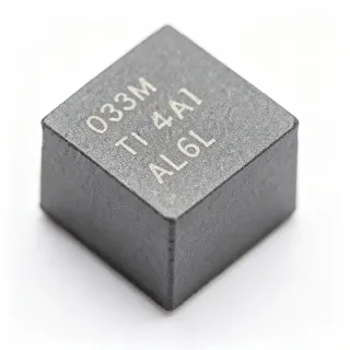
TPSM81033VCDR - 2A, 2.4MHz Boost Power Module | TI
MPN: TPSM81033VCDR ✓ Active| Qty | Unit Price | Extended |
|---|---|---|
| 1 | $2.05 | $2.05 |
| 10 | $1.85 | $18.50 |
| 100 | $1.62 | $162.00 |
| 500 | $1.42 | $710.00 |
| 1,000 | $1.28 | $1,280.00 |
TPSM81033VCDR Overview
A power module is a type of DC-DC converter that integrates the power inductor and MOSFETs of a switching regulator into a single surface-mount package, sitting within the broader hierarchy of power management ICs that also includes LDOs, buck converters, and controllers. By integrating magnetics, modules dramatically reduce solution size and simplify layout compared to discrete converter designs.
Key features include a 1.8V to 5.5V input voltage range, an adjustable 2.2V to 5.5V output voltage range (with fixed 5.0V output when FB is connected to AVIN), a 2A valley switching current limit, and integrated 0.43uH power inductor with excellent thermal performance. The device operates at 2.4MHz switching frequency using an adaptive constant on-time valley-current-control topology, enabling small external components and fast transient response.
The module offers two light-load modes selected via the MODE pin: automatic PFM mode for highest efficiency and forced PWM mode for fixed-frequency noise immunity. Protection features include 5.75V output overvoltage protection, output short-circuit protection, and thermal shutdown. A power good output supports power-rail monitoring and sequencing.
Typical applications include battery-powered smart devices, portable equipment, Li-ion cell to 5V conversion, and point-of-load boost rails in compact electronics where board space is constrained. The small 2.6mm x 2.5mm footprint suits wearables and handheld instrumentation.
Design consideration: because the current limit is a valley limit of 2A typical, verify peak inductor current under worst-case load, minimum input voltage, and maximum output power to avoid hitting current limit during load transients.
Drop-in alternatives for TPSM81033VCDR — same package, pin-to-pin compatible. Different-package parts requiring PCB rework are excluded.
Quick Comparison Tool — Select alternative parts for side-by-side comparison:
No drop-in alternatives available for this product.
Request AlternativesTPSM81033VCDR Maximum Ratings & Electrical Characteristics
| Topology | Synchronous Boost |
| Input Voltage Range | 1.8 V to 5.5 V |
| Output Voltage Range | 2.2 V to 5.5 V (fixed 5.0 V with FB tied to AVIN) |
| Output Current | 2 A (valley switching current limit, typical) |
| Switching Frequency | 2.4 MHz |
| Integrated Inductor | 0.43 uH (MagPack) |
| Control Topology | Adaptive constant on-time valley current control |
| Light Load Modes | Auto PFM / Forced PWM (MODE pin) |
| Output OVP | 5.75 V |
| Protection | Output OVP, output short-circuit, thermal shutdown |
| Power Good Output | Yes |
| Package | QFN-FCMOD (9), 2.6 mm x 2.5 mm |
| Mounting Type | Surface Mount |
| Packaging | Tape & Reel (VCDR suffix) |
TPSM81033VCDR Pin Configuration
| Pin 1 | AVIN — Analog supply input for control circuit; also connects to FB for fixed 5.0V output |
| Pin 2 | FB — Feedback input for output voltage adjustment; tie to AVIN for fixed 5.0V |
| Pin 3 | MODE — Light-load mode select: auto PFM or forced PWM |
| Pin 4 | PGOOD — Power good output flag |
| Pin 5 | GND — Ground |
| Pin 6 | SW — Switch node (integrated power stage) |
| Pin 7 | EN — Enable input |
| Pin 8 | VIN — Power stage input supply, 1.8 V to 5.5 V |
| Pin 9 | VOUT — Boosted output, 2.2 V to 5.5 V |
Typical Applications
TPSM81033VCDR is suitable for 6 applications: Battery-Powered Smart Devices, Portable Equipment Power Rails, Point-of-Load Boost for MCUs and Processors, Wearables and IoT Edge Nodes, Display and LED Bias Supplies, Industrial Compact Sensor Nodes.
Battery-Powered Smart Devices
The TPSM81033's 1.8V to 5.5V input range directly covers single-cell alkaline, NiMH, and Li-ion battery stacks, boosting to a regulated 2.2V to 5.5V rail for MCUs, displays, and sensors. The integrated 0.43uH MagPack inductor yields a 2.6mm x 2.5mm solution, critical in space-constrained smart devices. Auto PFM light-load mode via the MODE pin preserves efficiency during sleep states, while the power good output lets the host MCU verify rail validity before waking.
Recommended
Portable Equipment Power Rails
For handheld instruments and portable equipment powered by batteries or USB, the TPSM81033 generates a stable 5.0V rail (FB tied to AVIN) from a 1.8V to 5.5V source. The 2.4MHz switching frequency keeps ripple components above sensitive analog bands and allows small passives. Built-in 5.75V OVP, short-circuit protection, and thermal shutdown provide robustness against user faults such as output shorts, reducing external protection circuitry.
Recommended
Point-of-Load Boost for MCUs and Processors
When a system's main 3.3V or 1.8V rail cannot supply a high-voltage peripheral, the TPSM81033 provides a local boost to 5V for displays, LEDs, or sensor interfaces. Constant on-time valley current control delivers fast transient response at 2.4MHz, and forced PWM mode fixes the switching spectrum for noise-sensitive designs. The 2A valley current limit supports typical peripheral loads while the small footprint enables placement near the load.
Recommended
Wearables and IoT Edge Nodes
Wearable electronics demand minimum board area and efficient power conversion from small cells. The TPSM81033's MagPack integration removes external inductor placement, cutting solution height and area versus discrete boost designs. Auto PFM mode maximizes light-load efficiency for duty-cycled IoT sensors, and the power good output simplifies power-up monitoring of the boosted rail feeding BLE MCUs or sensor front ends in sub-1cm-class designs.
Recommended
Display and LED Bias Supplies
Boost converters commonly generate 5V or higher bias rails for small LCD panels and indicator LEDs in portable products. The TPSM81033's adjustable 2.2V to 5.5V output accommodates display analog and interface supplies. The high 2.4MHz switching frequency places switching harmonics well above visible-artifact bands, and thermal shutdown protects against sustained output shorts from flex-cable damage in compact hinge assemblies.
Recommended
Industrial Compact Sensor Nodes
Industrial 3.3V or 5V logic rails often need local boosting for RF modules, isolation supplies, or analog front ends. The TPSM81033 accepts up to 5.5V input and boosts to 5.5V with 2A valley limit, fitting within a minimal PCB area on dense sensor boards. Short-circuit and overvoltage protection improve field reliability, and forced PWM mode provides a fixed 2.4MHz spectrum, easing EMC pre-compliance in noisy factory environments.
Recommended
Recommended Products Summary
Engineering reference data for TPSM81033VCDR — comparison, design guidance, and compliance information.
Selection Guide
Comparison with Alternatives
| Parameter | This Product | TPS610981DSET | TPS61160DRVR | TPS62740DSSR |
|---|---|---|---|---|
| Package | QFN-FCMOD (9), 2.6x2.5mm | WSON-8 (DSE) - different | WSON-6 (DRV) - different | SON-12 (DSS) - different |
| Brand | Texas Instruments | Texas Instruments | Texas Instruments | Texas Instruments |
| Topology | Synchronous Boost | Synchronous Boost | Synchronous Boost (LED) | Buck |
| Integrated Inductor | Yes (0.43 uH MagPack) | No - external required | No - external required | No - external required |
| Module vs IC | Power module (inductor integrated) | Converter IC | Converter IC | Converter IC |
Key Differentiators
- Fully integrated magnetics (vs TPS610981DSET)
- Fixed 5.0V output with zero divider components (vs TPS61160DRVR)
- Dual light-load modes (vs TPS62740DSSR)
Design Notes
The 2A valley switching current limit is a valley limit, not a peak limit. At minimum input voltage (1.8V) and high boost ratios, peak inductor current can significantly exceed the valley limit. Compute worst-case peak current per TI datasheet equations across full load, temperature, and input range, and derate output power accordingly to avoid hitting current limit during load transients.
Although the power inductor is integrated, input and output ceramic capacitors must still be placed as close as possible to the VIN and VOUT pins. Follow the QFN-FCMOD (9) footprint and layout guidelines in the TI datasheet: solid ground pour on the layer beneath the module, and multiple thermal vias to the ground plane to exploit the MagPack package's excellent thermal performance.
Use the MODE pin deliberately: auto PFM gives best light-load efficiency for battery life, while forced PWM holds a fixed 2.4MHz spectrum for noise-sensitive analog or RF sections. Never leave the EN pin floating; drive it from a supervisor or GPIO for controlled startup, and use the PGOOD output to gate downstream rails in multi-rail sequencing.
Compliance Information
RoHS status per TI product page conventions for active TI modules; detailed REACH/halogen declarations available on TI.com product page. Not an automotive Q1 part.