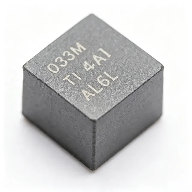
TPSM81033VCDR - 2A 2.4MHz Synchronous Boost Module | TI
MPN: TPSM81033VCDR ✓ Active| Qty | Unit Price | Extended |
|---|---|---|
| 1 | $2.15 | $2.15 |
| 10 | $1.93 | $19.30 |
| 100 | $1.66 | $166.00 |
| 500 | $1.42 | $710.00 |
| 1,000 | $1.21 | $1,210.00 |
TPSM81033VCDR Overview
A boost converter (step-up switching regulator) is a DC-DC converter that raises an input voltage to a higher regulated output by storing energy in an inductor and releasing it at higher voltage through a switching FET. Boost converters form part of the power management IC hierarchy and are essential wherever battery voltage is lower than the load rail, such as single-cell Li-ion or alkaline systems needing a 5V rail.
Key features include the integrated inductor enabled by MagPack technology, 2.4MHz switching frequency that allows tiny external components and fast transient response, fixed 5.0V output option by connecting FB to AVIN, selectable light-load mode (auto PFM or forced PWM) via the MODE pin, and power-good output. Protection features include 5.75V output overvoltage protection, output short-circuit protection, and thermal shutdown.
The device uses adaptive constant on-time valley-current-control topology, providing fast load transients and predictable behavior. Forced PWM mode trades light-load efficiency for constant switching frequency, important for noise-sensitive RF and analog rails.
Typical applications include smart devices and portable battery-powered equipment, RF power amplifiers needing a stable 5V from Li-ion cells, and OLED or display bias supplies. The tiny footprint and minimum external component count make it ideal for space-constrained wearables and IoT devices.
Design consideration: boost converter output current capability decreases as input voltage drops; verify the 2A valley current limit supports your load at minimum VIN, and follow the datasheet PCB layout for thermal performance of the exposed package.
Drop-in alternatives for TPSM81033VCDR — same package, pin-to-pin compatible. Different-package parts requiring PCB rework are excluded.
Quick Comparison Tool — Select alternative parts for side-by-side comparison:
TPS61230
✓ In Stock
$1.2 / Unit
View Datasheet →TPS610981DSER
✓ In Stock
$0.62 / Unit
View Datasheet →TPS61240
📋 Reference alternative (not in catalog)
TPS61322
📋 Reference alternative (not in catalog)
TPSM81033VCDR Maximum Ratings & Electrical Characteristics
| Topology | Synchronous Boost (Step-Up) |
| Input Voltage Range | 1.8 V to 5.5 V |
| Output Voltage Range | 2.2 V to 5.5 V |
| Fixed Output Option | 5.0 V (FB connected to AVIN) |
| Switch Current Limit | 2 A (typical, valley) |
| Switching Frequency | 2.4 MHz |
| Integrated Inductor | 0.43 uH (MagPack) |
| Control Topology | Adaptive constant on-time valley current control |
| Light Load Modes | Auto PFM or Forced PWM (MODE pin) |
| Power Good Output | Yes |
| Overvoltage Protection | 5.75 V output OVP |
| Short Circuit Protection | Yes |
| Thermal Shutdown | Yes |
| Package | QFN-FCMOD (9), 2.6 mm x 2.5 mm |
| Mounting Type | Surface Mount |
| RoHS Status | Compliant |
TPSM81033VCDR Pin Configuration
| Pin 1 | VIN — Switching input supply, connects to integrated inductor |
| Pin 2 | AVIN — Analog input supply; tie FB to AVIN for fixed 5.0V output |
| Pin 3 | GND — Ground |
| Pin 4 | EN — Enable input, active high |
| Pin 5 | FB — Feedback input for output voltage setting |
| Pin 6 | MODE — Mode select: auto PFM or forced PWM |
| Pin 7 | PG — Power good output (open drain) |
| Pin 8 | SS/TR — Soft start / tracking [DATA_NEEDED: confirm pin function] |
| Pin 9 | VOUT — Boost output voltage |
Typical Applications
TPSM81033VCDR is suitable for 6 applications: Single-Cell Li-Ion to 5V Rail, RF Power Amplifier Supply, Wearables and Smart Devices, Display and OLED Bias, IoT Sensor Nodes, Industrial Portable Instruments.
Single-Cell Li-Ion to 5V Rail
The TPSM81033VCDR converts a single Li-ion cell (2.7V-4.2V) to a stable 5V rail using its 1.8V-5.5V input range and fixed 5.0V output mode (FB tied to AVIN). The 2A valley current limit supports loads in the 1-1.5W class over the full battery discharge curve. Its integrated 0.43uH MagPack inductor at 2.4MHz switching keeps the solution within a few square millimeters, and auto PFM mode preserves standby battery life in portable systems.
Recommended
RF Power Amplifier Supply
RF PA stages require a clean, stiff supply; supply ripple directly modulates the transmitted signal. The TPSM81033VCDR's forced PWM mode holds the 2.4MHz switching frequency constant at light load, making output ripple predictable and easy to filter, while the power-good flag enables safe PA enable sequencing. The integrated inductor removes inductor selection risk, and 5.75V output OVP protects downstream RF components from runaway output during faults.
Recommended
Wearables and Smart Devices
Wearables demand the smallest possible power footprint. The TPSM81033VCDR's 2.6mm x 2.5mm QFN-FCMOD (9) MagPack package integrates the inductor, so the whole boost solution occupies minimal board area with only input/output capacitors and one FB resistor as external parts. The MODE pin lets designers trade light-load efficiency (auto PFM) against ripple cleanliness (forced PWM), and thermal shutdown plus short-circuit protection add robustness in compact, thermally constrained enclosures.
Recommended
Display and OLED Bias
OLED panels and small displays commonly need a boosted 4.5V-5.5V rail from a battery or low-voltage system rail. The TPSM81033VCDR covers 2.2V-5.5V output with a resistive divider on FB, and its 2.4MHz operation keeps the switching ripple above the display driver's sensitive band. Fast adaptive constant on-time control handles the load steps that occur when display brightness or refresh changes, minimizing visible flicker; the power-good output can gate the panel enable signal.
Recommended
IoT Sensor Nodes
Battery-powered IoT nodes spend most of their life in sleep, so light-load efficiency governs battery life. In auto PFM mode the TPSM81033VCDR reduces switching activity at light load, and its 1.8V input floor allows operation from two alkaline cells down to end-of-discharge. When the radio transmits, the adaptive constant on-time valley current control supplies fast load transients without large output droop, and the PG flag verifies rail validity before the MCU boots.
Recommended
Industrial Portable Instruments
Handheld test and measurement instruments need a regulated 5V logic and analog rail from 3-4 cell battery stacks. The TPSM81033VCDR's integrated protections (5.75V OVP, short-circuit protection, thermal shutdown) reduce external protection circuitry, important in instruments subject to probe shorts and rough handling. Forced PWM mode gives deterministic noise for precision analog front ends, and the pre-integrated power stage shortens qualification versus a discrete boost design.
Recommended
Recommended Products Summary
Engineering reference data for TPSM81033VCDR — comparison, design guidance, and compliance information.
Selection Guide
Comparison with Alternatives
| Parameter | This Product | TPS61230 | TPS610981DSER | TPS61322 |
|---|---|---|---|---|
| Package | QFN-FCMOD (9), 2.6 x 2.5 mm | SON-8 | SON-10 | VQFN-20 |
| Brand | Texas Instruments | Texas Instruments | Texas Instruments | Texas Instruments |
| Input Voltage Range | 1.8 V to 5.5 V | 2.3 V to 5.5 V | 0.7 V to 5.5 V | 2.4 V to 5.5 V |
| Integrated Inductor | Yes (0.43 uH MagPack) | No - external | No - external | No - external |
| Switching Frequency | 2.4 MHz | 2 MHz | Frequency-scaled PFM/PWM | 1.2 MHz / 2 MHz selectable |
| Light Load Mode | Auto PFM / Forced PWM (MODE pin) | PFM/PWM (PSAVE pin) | Optimized low-Iq PFM | Auto PFM / Forced PWM |
| Power Good Output | Yes | Yes (PGOOD) | No | Yes (PGOOD) |
| Solution Size | Smallest (module, inductor integrated) | IC + external inductor | IC + external inductor | IC + external inductor |
Key Differentiators
- Integrated 0.43uH MagPack inductor (vs TPS61230)
- Selectable auto PFM / forced PWM (vs TPS610981DSER)
- Lower input voltage floor (1.8V) (vs TPS61322)
Design Notes
Place the input capacitor as close as possible to VIN/AVIN and the output capacitor close to VOUT/GND, per the TI TPSM81033 datasheet layout section. Because the 0.43uH inductor and power FETs are integrated in the QFN-FCMOD (9) package, the main layout concern is minimizing loop area on the input capacitor and providing adequate copper on GND for thermal performance of the 2.6mm x 2.5mm body.
Boost converters draw high input current at low VIN: with a 2A valley current limit, available output power falls as input voltage drops toward 1.8V. Compute the available load current at minimum battery voltage, add margin, and size the input source impedance (battery, traces, connector) so VIN does not sag into current limit during transmit or burst loads.
Do not exceed 5.5V on VIN/AVIN; the internal OVP clamps output at 5.75V but input transients can damage the part. If a fixed 5.0V output is used (FB to AVIN), confirm your load tolerates the 5.0V nominal and use the MODE pin deliberately: forced PWM raises noise immunity but increases quiescent draw at light load, reducing battery life.
Compliance Information
RoHS compliant per TI/DigiKey product listings. REACH and halogen-free status not stated in provided data.






