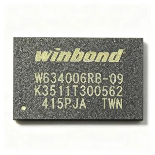
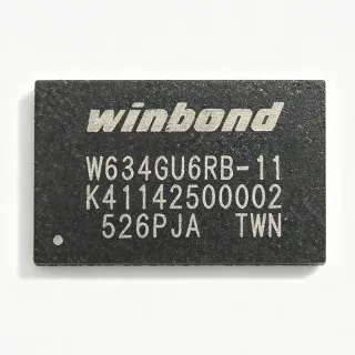
W971GG6NB-25 TR - 1Gbit DDR2 SDRAM 400MHz | Winbond
MPN: W971GG6NB-25 TR ✓ Active| Qty | Unit Price | Extended |
|---|---|---|
| 1 | $6.91 | $6.91 |
| 10 | $6.56 | $65.60 |
| 100 | $6.22 | $622.00 |
| 500 | $5.91 | $2,955.00 |
| 1,000 | $5.62 | $5,620.00 |
W971GG6NB-25 TR Overview
DDR2 SDRAM (Double Data Rate Type Two Synchronous Dynamic Random Access Memory) is a class of volatile memory that transfers data on both rising and falling edges of the clock, doubling effective bandwidth compared to single data rate SDRAM. Within the memory hierarchy, it sits as a main-system-memory technology between DDR1 and DDR3, and remains widely used in cost-sensitive embedded and industrial designs that do not require DDR3/DDR4 bandwidth.
Key features include a JEDEC-compliant SSTL_18 interface operating from a single 1.8V supply, 8 internal banks with burst lengths of 4 or 8, and on-die termination support. The x16 organization simplifies 16-bit and 32-bit memory subsystems by reducing required bus width and controller complexity.
Architecturally, the device achieves high-speed transfer rates up to DDR2-800 class performance, using a 4n prefetch architecture that internally runs at half the external data rate. Posted CAS additive latency and programmable CAS latency help the memory controller schedule reads efficiently and minimize command bus contention.
Typical applications include set-top boxes, networking equipment, industrial HMI panels, digital television, and embedded processor memory subsystems for SoCs requiring DDR2 interfaces.
Design consideration: ensure SSTL_18 signal integrity with proper on-die or external termination and adhere to datasheet trace-length matching rules for the 84-TFBGA ballout; refresh (64 ms) must be scheduled per controller settings.
This page synthesizes distributor pricing, drop-in family alternatives, and practical DDR2 design notes not consolidated in the manufacturer datasheet.
Drop-in alternatives for W971GG6NB-25 TR — same package, pin-to-pin compatible. Different-package parts requiring PCB rework are excluded.
Quick Comparison Tool — Select alternative parts for side-by-side comparison:
W971GG6NB-25
✅ Drop-In📋 Reference alternative (not in catalog)
W971GG6NB-25 TR
✅ Drop-In✓ In Stock
$5.62 / Unit
View Datasheet →W971GG6NB-6 TR
✅ Drop-In ⚠️ 参数待验证📋 Reference alternative (not in catalog)
W971GG6NB-18 TR
✅ Drop-In ⚠️ 参数待验证📋 Reference alternative (not in catalog)
W971GG6SB-25 TR
✅ Drop-In ⚠️ 参数待验证📋 Reference alternative (not in catalog)
W971GG6NB-25 TR Maximum Ratings & Electrical Characteristics
| Memory Type | SDRAM - DDR2 |
| Memory Size | 1 Gbit |
| Organization | 64M x 16 (8,388,608 words x 8 banks x 16 bits) |
| Clock Frequency | 400 MHz |
| Access Time | 57.5 ns |
| Write Cycle Time | 15 ns |
| Interface | SSTL_18 |
| Supply Voltage | 1.8 V |
| Number of Banks | 8 |
| Data Rate | DDR2-800 |
| Package | 84-TFBGA (8 x 12.5 mm) |
| Mounting Type | Surface Mount |
| Packaging | Tape & Reel (TR) |
| RoHS Status | Compliant (all Winbond packaging RoHS compliant per manufacturer) |
W971GG6NB-25 TR 84-tfbga (8 x 12.5 mm) Pin Configuration Guide
Pin configuration for W971GG6NB-25 TR (84-tfbga (8 x 12.5 mm) package). This digital IC includes GPIO, communication interfaces (UART, SPI, I2C), and power pins. Refer to the manufacturer datasheet for alternate pin functions and configuration options. Essential for embedded system design and PCB layout.

No detailed pinout data available for W971GG6NB-25 TR.
Refer to the datasheet for full pin configuration.
Typical Applications
W971GG6NB-25 TR is suitable for 6 applications: Set-Top Boxes and Digital TV, Industrial HMI and Control Panels, Networking Equipment, Embedded SoC Main Memory, Automotive Infotainment (Non-Safety) Retrofits, Test and Measurement Instruments.
Set-Top Boxes and Digital TV
The W971GG6NB-25 TR fits set-top box and digital TV platforms whose SoCs expose DDR2 memory controllers with 16-bit buses. Its 64M x 16 organization lets one chip serve the full 16-bit channel, cutting component count and PCB layers versus x8 designs, while DDR2-800 class bandwidth (400 MHz clock, double data rate) comfortably sustains video decode buffering and channel-change caching. Because the device runs on a single 1.8V SSTL_18 supply, power budgeting is straightforward for always-on consumer boxes. Board designers should place the TFBGA within the controller's fly-by length-matching rules and enable on-die or external termination to keep signal integrity at speed. The result is a cost-optimized main memory subsystem for broadcast and streaming products.
Recommended
Industrial HMI and Control Panels
Industrial human-machine interface panels and PLC front ends typically need 128 MB to 512 MB of working memory for graphics stacks and protocol stacks - exactly the range a 1 Gbit DDR2 device covers. The W971GG6NB-25 TR's JEDEC-standard SSTL_18 interface connects directly to industrial-grade SoCs and FPGAs with DDR2 hard controllers, and its 8-bank architecture supports the random-access patterns of GUI frame buffers and logging buffers. Winbond's long-lifecycle DDR/SDR line and broad distribution stocking (DigiKey, Mouser, LCSC) ease industrial BOM continuity. Designers should confirm the datasheet temperature range against cabinet conditions and schedule controller refresh at the JEDEC 64 ms interval, derating for high ambient temperatures.
Recommended
Networking Equipment
Edge routers, switches, and wireless access points use DDR2 as packet-buffer and route-table memory. The W971GG6NB-25 TR's 400 MHz double-data-rate interface delivers DDR2-800 class bandwidth in a compact 84-TFBGA (8 x 12.5 mm) footprint, fitting the dense memory arrays typical of line-card designs. The x16 organization maps neatly onto 16-bit and 32-bit network processor buses, halving chip count compared to x8 parts. Burst lengths of 4 or 8 let the memory controller match packet sizes, improving effective throughput. When multiple DRAMs share a bus, follow the datasheet termination guidance for SSTL_18 nets and keep DQS-DQ skews within spec to sustain error-free operation at full clock rate.
Recommended
Embedded SoC Main Memory
Many embedded ARM, MIPS, and PowerPC SoCs still ship with DDR2-only memory controllers, making the W971GG6NB-25 TR a natural main-memory choice. One device provides 128 MByte of working memory - sufficient for Linux-based firmware with graphics or network services - via a simple point-to-point or short multi-drop SSTL_18 bus. The 1.8V single-rail supply simplifies power-tree design alongside 3.3V and 1.2V logic rails. Firmware teams should configure the controller for the -25 speed grade's CAS latency and 57.5 ns access timing and verify boot-time memory training against Winbond's timing tables. Tape & Reel packaging supports high-volume automated SMT placement on production lines.
Recommended
Automotive Infotainment (Non-Safety) Retrofits
Aftermarket head units and non-safety infotainment modules built on DDR2-generation media processors use 1 Gbit DDR2 x16 parts as framebuffer and application memory. The W971GG6NB-25 TR supplies DDR2-800 class bandwidth adequate for navigation rendering and audio buffering, and the 84-TFBGA (8 x 12.5 mm) package suits the compact two-sided boards common in 1-DIN chassis. Note that this standard-grade part is not AEC-Q100 qualified; it suits aftermarket and non-safety roles, not under-hood or safety-critical nodes. In-vehicle thermal environments demand a temperature-range review and possible conformal coating, plus refresh scheduling derated for elevated cabin temperatures.
Recommended
Test and Measurement Instruments
Bench instruments, data loggers, and compact test modules use DDR2 DRAM for sample buffering and result storage. The W971GG6NB-25 TR's 128 MByte capacity and 400 MHz DDR2 interface provide enough bandwidth to stream digitizer data while the host CPU processes previous blocks. The SSTL_18 interface ties directly into FPGA memory controllers (Xilinx and Intel hard/soft DDR2 controllers are mature), shortening firmware development. For high-accuracy instruments, isolate DRAM power rails from analog supplies and follow the datasheet layout rules for DQS strobe routing to minimize capture jitter. Tape & Reel delivery suits contract manufacturers building instrument families on a common memory footprint.
Recommended
Recommended Products Summary
Engineering reference data for W971GG6NB-25 TR — comparison, design guidance, and compliance information.
Selection Guide
Comparison with Alternatives
| Parameter | This Product | W971GG6NB-25 | W971GG6NB-6 TR | W971GG6NB-18 TR | W971GG6SB-25 TR |
|---|---|---|---|---|---|
| Package | 84-TFBGA (8x12.5 mm) | 84-TFBGA (8x12.5 mm) - same | 84-TFBGA (8x12.5 mm) - same | 84-TFBGA (8x12.5 mm) - same | 84-TFBGA (8x12.5 mm) - same |
| Brand | Winbond Electronics | Winbond Electronics | Winbond Electronics | Winbond Electronics | Winbond Electronics |
| Memory Size | 1 Gbit | 1 Gbit | 1 Gbit | 1 Gbit | 1 Gbit |
| Organization | 64M x 16 | 64M x 16 | 64M x 16 | 64M x 16 | 64M x 16 |
| Speed Grade | -25 (400 MHz clock, 57.5 ns access) | -25 (identical) | -6 (faster bin) | -18 bin | -25 (die revision SB) |
| Interface / Supply | SSTL_18, 1.8 V | SSTL_18, 1.8 V | SSTL_18, 1.8 V | SSTL_18, 1.8 V | SSTL_18, 1.8 V |
| Packaging | Tape & Reel (TR) | Tray | Tape & Reel | Tape & Reel | Tape & Reel |
Key Differentiators
- Identical die in Tape & Reel for automated assembly (vs W971GG6NB-25 (tray))
- JEDEC-compliant DDR2 with broad SoC support (vs Newer DDR3/DDR4 parts)
- Speed-grade upgrade path within the same footprint (vs W971GG6NB-6 TR)
Design Notes
Route the SSTL_18 address/command bus as a controlled-impedance (~50 ohm single-ended) topology with series termination at the controller, and match DQ/DQS trace lengths per the Winbond W971GG6NB datasheet layout guidelines. Keep DQS-DQ skew minimal and reference all DDR2 nets to a solid ground plane; avoid routing DDR2 signals across plane splits. At 400 MHz clock rates, on-die termination or external SSTL_18 termination resistors are essential to suppress reflections on the 84-TFBGA ballout.
The device operates from a single 1.8V rail for both core and SSTL_18 I/O; provide separate bulk and local decoupling (bulk capacitor near the regulator plus multiple 0.1 uF ceramics at VDD/VDDQ balls of the 84-TFBGA). DDR2 supply current is bursty and data-dependent, so size the regulator for peak read/write bursts, not average current, and add a small ferrite bead only if rail noise coupling to sensitive analog circuitry is observed. Verify VTT termination rail sizing if external termination is used.
Verify the memory controller is configured for the -25 speed grade timing (400 MHz clock, correct CAS latency per the Winbond datasheet speed-bin table) before qualification; substituting a different speed-grade suffix (-6, -18) requires re-checking the controller timing registers. Also schedule refresh at the datasheet-specified interval with temperature-derating if the environment exceeds nominal, and remember the TR suffix is packaging only - the die is identical to the tray version.
Compliance Information
Per Winbond official purchasing guide: all Winbond Flash/memory products use RoHS-compliant, Halogen-Free packaging. Parts with G in the 13th character of the part number are manufactured using renewable energy with identical specifications.