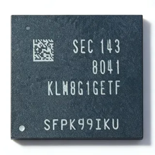
W9812G6KH-6I TR - 128Mb SDRAM 166MHz 3.3V | Winbond
MPN: W9812G6KH-6I TR ✓ Active| Qty | Unit Price | Extended |
|---|---|---|
| 1 | $1.45 | $1.45 |
| 10 | $1.3 | $13.00 |
| 100 | $1.12 | $112.00 |
| 500 | $0.98 | $490.00 |
| 1,000 | $0.86 | $860.00 |
W9812G6KH-6I TR Overview
An SDRAM is a type of DRAM that synchronizes all address, data, and control signals to a system clock, allowing pipelined burst accesses at the clock edge. Within the memory hierarchy, SDRAM sits above asynchronous DRAM (FPM/EDO) and below DDR generations, and remains the standard volatile memory choice for microcontroller, DSP, and FPGA systems that lack DDR controllers. The W9812G6KH family belongs to the broader DRAM and volatile memory IC category.
Key features include a 166 MHz clock rate at CL3 (-6I speed grade), a data bandwidth of up to 200M words per second, four internal banks with interleaved operation to hide precharge and row-to-row delays, and programmable CAS latency and burst lengths (1, 2, 4, 8, or full page). The industrial temperature rating (-40C to +85C) makes the -6I grade suitable for harsh environments.
Technically, the device uses a synchronous interface with row and bank activation commands, auto-refresh and self-refresh modes, and auto/precharge options per the standard SDRAM command set. Power is supplied at a nominal 3.3V with LVTTL logic levels, and clock-enable (CKE) support allows power-down for reduced standby current.
Typical applications include embedded controller buffering, network equipment line-card memory, industrial HMI frame buffers, and FPGA-based data acquisition systems where an SDR SDRAM controller is already implemented.
A key design consideration is refresh budgeting: allocate tRFC and 4096 refresh cycles per 64 ms into your controller scheduling, and terminate clock and address lines appropriately at 166 MHz to maintain signal integrity on a 54-pin TSOP-II footprint.
This page synthesizes distributor pricing, drop-in alternatives across Winbond and ISSI, and practical design notes not found in the manufacturer datasheet.
Drop-in alternatives for W9812G6KH-6I TR — same package, pin-to-pin compatible. Different-package parts requiring PCB rework are excluded.
Quick Comparison Tool — Select alternative parts for side-by-side comparison:
W9812G6KH-6I
✅ Drop-In📋 Reference alternative (not in catalog)
W9812G6KH-5I
✅ Drop-In📋 Reference alternative (not in catalog)
W9812G6KH-75
✅ Drop-In📋 Reference alternative (not in catalog)
W9812G6JH-6
✅ Drop-In📋 Reference alternative (not in catalog)
IS42S16800F-6TLI
✅ Drop-In📋 Reference alternative (not in catalog)
W9812G6KH-6I TR Maximum Ratings & Electrical Characteristics
| Memory Type | SDR SDRAM |
| Memory Size | 128 Mbit |
| Organization | 8M x 16 (2M words x 4 banks x 16 bits) |
| Clock Frequency | 166 MHz |
| Clock Cycle Time | 5 ns (-6 speed grade) |
| CAS Latency | CL3 |
| Supply Voltage | 3.3 V |
| Interface Type | LVTTL |
| Number of Banks | 4 |
| Refresh | 4096 refresh cycles per 64 ms |
| Burst Length | 1, 2, 4, 8, full page |
| Operating Temperature | -40C to +85C (industrial) |
| Package | 54-TSOP II |
| Mounting Type | Surface Mount |
| Packaging | Tape & Reel (TR) |
| Data Bandwidth | Up to 200M words per second |
| Speed Grades in Family | -5, -5I, -5J, -6, -6I, -6J, -75 |
W9812G6KH-6I TR 54-tsop ii Pin Configuration Guide
Pin configuration for W9812G6KH-6I TR (54-tsop ii package). This digital IC includes GPIO, communication interfaces (UART, SPI, I2C), and power pins. Refer to the manufacturer datasheet for alternate pin functions and configuration options. Essential for embedded system design and PCB layout.

No detailed pinout data available for W9812G6KH-6I TR.
Refer to the datasheet for full pin configuration.
Typical Applications
W9812G6KH-6I TR is suitable for 6 applications: Embedded Controller System Memory, Industrial HMI and TFT Display Frame Buffer, FPGA Data Acquisition Buffering, Networking Equipment Line-Card Buffer Memory, Medical and Instrumentation Data Logging, POS Terminals and Consumer Smart Devices.
Embedded Controller System Memory
The W9812G6KH-6I TR provides 32 MB of external volatile memory for 16/32-bit MCUs and MPUs whose on-chip SRAM is insufficient for RTOS stacks, network buffers, or file systems. Its 166 MHz CL3 timing and standard JEDEC command set work with common MCU external memory controllers, while the 3.3V LVTTL interface connects directly without level shifters. Burst lengths of 1, 2, 4, 8, and full page let the controller match burst behavior to cache-line or DMA-block sizes, and four internal banks hide row-activation latency during sequential accesses. The industrial -40C to +85C rating keeps the part valid in uncontrolled factory-floor environments. Estimated benefit: up to 200M words per second bandwidth via 16-bit bursts at full clock rate.
Recommended
Industrial HMI and TFT Display Frame Buffer
Graphic HMIs with TFT panels of 4.3 to 10.1 inches require a dedicated frame buffer that on-chip SRAM cannot provide. The W9812G6KH-6I TR, with 128Mbit (16 MB x 8-bit pixels or 8 MB x 16-bit pixels) capacity, stores multiple full-frame buffers and lets the LCD DMA engine fetch pixel data at line rate while the CPU draws to a second buffer, eliminating tearing through double buffering. Its 166 MHz clock comfortably covers 800x480 resolution refresh bandwidth, and burst-8 accesses align with LCD FIFO prefetch depths. The TSOP-II-54 package keeps the memory low-profile behind the display. Self-refresh mode retains contents during low-power standby of the HMI.
Recommended
FPGA Data Acquisition Buffering
FPGA-based acquisition systems (oscilloscope front ends, industrial recorders, sensor loggers) need deep buffering between high-speed ADCs and slower host interfaces. The W9812G6KH-6I TR provides 32 MB of ping-pong buffering; at 166 MHz with a 16-bit bus it sustains an estimated 333 MB/s peak, enough to absorb bursts from 50-100 MSPS ADCs when writes are grouped into full-page bursts. Standard SDRAM controller IP on Xilinx, Intel, and Lattice fabrics drives the JEDEC command interface directly at 3.3V. Four-bank interleaving masks tRCD and tRP during alternating bank access, and the industrial temperature grade suits bench-to-field deployment. Budget 15.625 us worst-case refresh interruptions in your data-stream design.
Recommended
Networking Equipment Line-Card Buffer Memory
Ethernet switches, industrial gateways, and telecom line cards use external SDRAM for packet buffering, descriptor rings, and statistics counters. The W9812G6KH-6I TR delivers up to 200M words per second of bandwidth, sufficient for Fast Ethernet line-rate forwarding with headroom for management CPU traffic. Its four-bank architecture supports simultaneous read and write streams on alternating banks, matching the dual-FIFO pattern of packet engines, while full-page bursts maximize utilization on large jumbo frames. The -40C to +85C rating covers unventilated telecom cabinets, and the JEDEC-standard footprint enables dual-sourcing with the ISSI IS42S16800F-6TLI for supply resilience.
Recommended
Medical and Instrumentation Data Logging
Benchtop medical devices, patient monitors, and laboratory instruments accumulate waveforms and logs in local volatile memory before upload. The W9812G6KH-6I TR stores an estimated 32 MB of samples (16 million 16-bit readings), enough for hours of multi-channel physiological data at typical sampling rates. Its deterministic SDRAM command timing simplifies validation under IEC 60601-adjacent software processes, and the industrial range covers cold-chain and ambulance environments at -40C. Self-refresh preserves buffered data through brief power transitions while backup capacitors discharge, an estimated tens of milliseconds to hundreds of milliseconds depending on rail sizing. A battery-backed supervisor should assert CKE and clock-stop before rail collapse.
Recommended
POS Terminals and Consumer Smart Devices
Point-of-sale terminals, ticket machines, and smart retail devices pair application processors with external SDRAM for GUI, printer spooling, and transaction buffers. The W9812G6KH-6I TR offers a mature, low-cost 32 MB expansion with 166 MHz performance adequate for QVGA-to-WVGA GUIs and receipt image handling. The TR tape-and-reel format supports high-volume automated placement, and the 54-TSOP-II package has a long industry footprint with second sources. CKE-gated power-down and self-refresh modes reduce standby drain in battery/UPS-backed terminals. Estimated typical active current is in the tens of milliamps range at 3.3V, so a 500 mA-class 3.3V regulator covers both memory and controller comfortably.
Recommended
Recommended Products Summary
Engineering reference data for W9812G6KH-6I TR — comparison, design guidance, and compliance information.
Selection Guide
Comparison with Alternatives
| Parameter | This Product | W9812G6KH-6I | W9812G6KH-5I | W9812G6JH-6 | IS42S16800F-6TLI |
|---|---|---|---|---|---|
| Package | 54-TSOP II | 54-TSOP II - same | 54-TSOP II - same | 54-TSOP II - same | 54-TSOP II - same |
| Brand | Winbond Electronics | Winbond Electronics | Winbond Electronics | Winbond Electronics | ISSI |
| Memory Size / Organization | 128 Mbit, 8M x 16 (4 banks) | 128 Mbit, 8M x 16 | 128 Mbit, 8M x 16 | 128 Mbit, 8M x 16 | 128 Mbit, 8M x 16 |
| Clock Speed | 166 MHz (6 ns, CL3) | 166 MHz (CL3) | 200 MHz class (5 ns) | 166 MHz (CL3) | 166 MHz (CL3) |
| Supply Voltage | 3.3 V | 3.3 V | 3.3 V | 3.3 V | 3.3 V |
| Operating Temperature | -40C to +85C (industrial) | -40C to +85C | -40C to +85C | 0C to +70C (commercial) | -40C to +85C |
| Interface | LVTTL | LVTTL | LVTTL | LVTTL | LVTTL |
Key Differentiators
- Industrial temperature rating at commodity pricing (vs W9812G6JH-6)
- Cost-optimized speed selection (vs W9812G6KH-5I)
- Cross-brand second source availability (vs IS42S16800F-6TLI)
Design Notes
At 166 MHz, treat the SDRAM bus as a transmission-line system. Keep CLK, CKE, and command/address traces length-matched within the class requirements of your FPGA/MCU controller, and place a 22-33 ohm series resistor near the driver on CLK to control ringing. Route the 16-bit data bus as a matched group to DQM signals. On a two-layer board, keep TSOP-II-54 stubs short; a four-layer stack with a solid ground plane is strongly preferred for full-speed operation per Winbond datasheet layout guidance.
Decouple each supply pin pair with 0.1 uF ceramic capacitors placed within 2 mm of the TSOP-II-54 pins, plus at least 10 uF bulk capacitance per device. Estimated: SDRAM peak transient currents during bank activation can reach several hundred milliamps for a few nanoseconds, so low-ESR local decoupling prevents VDD droop that would violate VIH levels. Power the device from a clean 3.3V rail; a dedicated LDO or well-filtered DC-DC output is preferred. Ensure VDDQ (I/O supply) and VDD rails are tied per datasheet schematic recommendations.
Do not forget the refresh budget: 4096 auto-refresh cycles must complete every 64 ms, an average interval of 15.625 us. Controllers that starve refresh during long full-page bursts will silently corrupt data, typically showing bit-rot patterns in bank-corner addresses. Also configure the mode register correctly at initialization: CAS latency 3 and the intended burst length must match your controller timing model. Finally, note that the third-party mislabeling of this part as DDR3 (seen on some aggregator sites) is wrong - it is single-data-rate SDRAM and must never be socketed into DDR3 footprints.
The 54-TSOP-II package dissipates little power at 3.3V - estimated a few hundred milliwatts worst case at 166 MHz continuous access - so no heatsink or copper-pour strategy beyond standard ground plane connection is required. However, ensure ambient air inside sealed enclosures keeps junction temperature within the -40C to +85C industrial range; combine the SDRAM self-heat with adjacent regulator dissipation when estimating internal enclosure temperature.
Compliance Information
RoHS compliance per distributor listings for current Winbond W9812G6KH production. REACH, halogen-free, and conflict-minerals status not stated in the provided data.