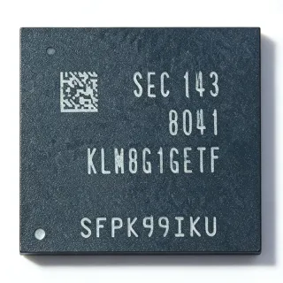
W9825G6KH-6 - 256Mb 166MHz SDR SDRAM | Winbond | 54-TSOP II
MPN: W9825G6KH-6 ✓ Active| Qty | Unit Price | Extended |
|---|---|---|
| 1 | $4.79 | $4.79 |
| 10 | $4.45 | $44.50 |
| 100 | $4.15 | $415.00 |
| 500 | $3.9 | $1,950.00 |
| 1,000 | $3.65 | $3,650.00 |
W9825G6KH-6 Overview
SDRAM (Synchronous Dynamic Random Access Memory) is a class of DRAM synchronized to the system clock, allowing a memory controller to execute commands - activate, read, write, precharge - on defined clock edges rather than asynchronously. Within the memory hierarchy, SDRAM sits between on-chip SRAM caches and non-volatile storage such as NOR/NAND flash, providing megabytes of fast working memory for processors that lack sufficient internal RAM.
Key features of the W9825G6KH include a x16 organization (16,777,216 words x 16 bits), four internal banks with burst lengths of 1, 2, 4, 8, or full-page, and programmable CAS latency. The device complies with the personal computer industrial standard for SDRAM and is sorted into speed grades -5, -5I, -6, -6I, -6J, -6L, -75, 75J and 75L per the Winbond datasheet, so the -6 grade designates the commercial-temperature 166 MHz version.
Technically, the W9825G6KH uses a four-bank architecture with row and column addressing (12 row address lines, 8 column address lines for x16), bank activate/read/write/precharge commands, and auto-refresh with self-refresh entry for low-power standby. Two DQM (data mask) pins enable byte-lane masking on the 16-bit bus, and mode register programming selects burst length, burst type, and CAS latency.
Typical applications include external memory expansion for STM32, NXP i.MX RT, and other MCUs/MPUs with SDRAM controllers, industrial HMI display frame buffers, network appliance buffers, and data acquisition buffering. Its 3.3V interface and standard TSOP II footprint keep board-level integration simple.
Design consideration: maintain proper signal integrity by keeping clock, DQM, and address traces length-matched, and implement the full auto-refresh schedule required by the controller to prevent data loss.
This page synthesizes distributor pricing, verified drop-in alternatives, and practical design notes not found in the manufacturer datasheet.
Drop-in alternatives for W9825G6KH-6 — same package, pin-to-pin compatible. Different-package parts requiring PCB rework are excluded.
Quick Comparison Tool — Select alternative parts for side-by-side comparison:
W9825G6KH-6I
✅ Drop-In📋 Reference alternative (not in catalog)
W9825G6KH-6J
✅ Drop-In ⚠️ 参数待验证📋 Reference alternative (not in catalog)
W9825G6KH-5
✅ Drop-In ⚠️ 参数待验证📋 Reference alternative (not in catalog)
MT48LC16M16A2P-6A IT:G
✅ Drop-In📋 Reference alternative (not in catalog)
W9825G6KH-6 Maximum Ratings & Electrical Characteristics
| Memory Type | SDRAM - SDR (Synchronous DRAM) |
| Memory Capacity | 256 Mbit (32 MB) |
| Organization | 16M x 16 (x16) |
| Clock Speed | 166 MHz (-6 speed grade) |
| Access Time | 5 ns |
| Interface | Parallel |
| Supply Voltage | 3.3 V |
| Number of Banks | 4 |
| Data Bandwidth | Up to 200M words per second |
| Burst Length | 1, 2, 4, 8, full page |
| Refresh | Auto-refresh and self-refresh |
| Package | 54-TSOP II |
| Mounting Type | Surface Mount |
| Operating Temperature | 0C to +70C (commercial grade) |
| Speed Grades Available | -5, -5I, -6, -6I, -6J, -6L, -75, 75J, 75L |
W9825G6KH-6 Pin Configuration
| Pin 1 | VDD — Power supply (3.3V) |
| Pin 2 | DQ0 — Data input/output bit 0 |
| Pin 3 | VDDQ — DQ power supply |
| Pin 4 | DQ1 — Data input/output bit 1 |
| Pin 5 | DQ2 — Data input/output bit 2 |
| Pin 6 | VSSQ — DQ ground |
| Pin 7 | DQ3 — Data input/output bit 3 |
| Pin 8 | DQ4 — Data input/output bit 4 |
| Pin 9 | VDD — Power supply (3.3V) |
| Pin 10 | DQ5 — Data input/output bit 5 |
| Pin 11 | DQ6 — Data input/output bit 6 |
| Pin 12 | VSSQ — DQ ground |
| Pin 13 | DQ7 — Data input/output bit 7 |
| Pin 14 | VDDQ — DQ power supply |
| Pin 15 | LDQM — Low-byte data input/output mask |
| Pin 16 | WE — Write enable command input |
| Pin 17 | CAS — Column address strobe |
| Pin 18 | RAS — Row address strobe |
| Pin 19 | CS — Chip select |
| Pin 20 | NC — Not connected (per datasheet) |
| Pin 21 | BA0 — Bank address 0 |
| Pin 22 | BA1 — Bank address 1 |
| Pin 23 | A0 — Address input bit 0 |
| Pin 24 | A1 — Address input bit 1 |
| Pin 25 | A2 — Address input bit 2 |
| Pin 26 | A3 — Address input bit 3 |
| Pin 27 | VDD — Power supply (3.3V) |
| Pin 28 | A4 — Address input bit 4 |
| Pin 29 | A5 — Address input bit 5 |
| Pin 30 | A6 — Address input bit 6 |
| Pin 31 | A7 — Address input bit 7 |
| Pin 32 | VSS — Ground |
| Pin 33 | A8 — Address input bit 8 (column address for x16) |
| Pin 34 | A9 — Address input bit 9 (column address for x16) |
| Pin 35 | A10 — Address bit 10 / auto-precharge select |
| Pin 36 | A11 — Address input bit 11 |
| Pin 37 | A12 — Address input bit 12 |
| Pin 38 | CKE — Clock enable (active high; low enters self-refresh/power-down) |
| Pin 39 | CLK — System clock input |
| Pin 40 | NC — Not connected (per datasheet) |
| Pin 41 | DQ8 — Data input/output bit 8 |
| Pin 42 | VDDQ — DQ power supply |
| Pin 43 | DQ9 — Data input/output bit 9 |
| Pin 44 | DQ10 — Data input/output bit 10 |
| Pin 45 | VSSQ — DQ ground |
| Pin 46 | DQ11 — Data input/output bit 11 |
| Pin 47 | DQ12 — Data input/output bit 12 |
| Pin 48 | VDD — Power supply (3.3V) |
| Pin 49 | DQ13 — Data input/output bit 13 |
| Pin 50 | DQ14 — Data input/output bit 14 |
| Pin 51 | VSSQ — DQ ground |
| Pin 52 | DQ15 — Data input/output bit 15 |
| Pin 53 | VSS — Ground |
| Pin 54 | UDQM — High-byte data input/output mask |
Typical Applications
W9825G6KH-6 is suitable for 6 applications: MCU/MPU External Memory Expansion, Industrial HMI and Display Frame Buffers, Networking and Communication Equipment, Data Acquisition and Test Instruments, Audio and Voice Processing, Legacy SDRAM Replacement and Last-Time-Buy Bridging.
MCU/MPU External Memory Expansion
The W9825G6KH-6 is the de-facto standard external RAM for STM32F4/F7/H7 (FMC), NXP i.MX RT, and similar controllers whose on-chip SRAM is insufficient for application data. Its 3.3V parallel interface, 16-bit data bus, and standard SDR SDRAM command set (ACTIVATE, READ, WRITE, PRECHARGE, AUTO REFRESH) map directly onto vendor SDRAM controllers with only timing-register configuration. At 166 MHz with a 16-bit bus it delivers up to 200M words per second of bandwidth - roughly 332 MB/s - enough for demanding middleware such as TCP/IP stacks, USB host buffering, and file systems. Configure CAS latency and refresh rate (64 ms/8192 rows) in the controller, and the four-bank architecture reduces row-miss penalties in mixed read/write workloads.
Recommended
Industrial HMI and Display Frame Buffers
TFT LCD modules of 4.3 to 10.1 inches at resolutions up to 800x480 RGB565 require a contiguous frame buffer of about 750 KB per frame; the W9825G6KH-6 provides 32 MB, enough for double or triple buffering plus graphics layers. Its deterministic SDR timing lets LTDC-style display controllers read the buffer continuously without DMA starvation, and the 200M word/s bandwidth supports smooth 60 fps updates with GUI engines such as TouchGFX. The commercial 0C to +70C rating suits indoor HMI panels, while the -6I variant covers outdoor or unconditioned factory environments. Self-refresh mode retains the framebuffer content during low-power standby, and the 3.3V rail is typically already present in display subsystems.
Recommended
Networking and Communication Equipment
Routers, industrial Ethernet switches, and gateways need packet buffers that tolerate bursty ingress traffic; the W9825G6KH-6's 256Mbit capacity and four-bank organization allow packet descriptors and payload buffering to be spread across banks, reducing row-conflict stalls. The 16-bit bus with two DQM byte-mask pins enables efficient partial-packet writes at the byte-lane level. With 166 MHz operation the device sustains line-rate forwarding for 100 Mbps-class systems with headroom, and auto-refresh scheduling can be aligned to idle slots to hide refresh latency. Its long-term availability from Winbond is a key advantage over discontinued SDRAMs in equipment with 10+ year service lives.
Recommended
Data Acquisition and Test Instruments
Multi-channel data acquisition systems buffer ADC sample streams before offload to flash or host interfaces. The W9825G6KH-6's 32 MB capacity stores millions of 16-bit samples - for example, 16 million single-channel readings - while the 166 MHz bus absorbs sustained sample rates from parallel ADCs without overflow. The x16 organization matches 12/16-bit ADC output widths, and DQM masking simplifies sample packing. Low latency (5 ns access) supports trigger-scoped capture-and-hold workflows. In bench instruments, the commercial temperature rating is adequate, and the TSOP II package reflows on standard assembly lines. Pair with a CPLD or FPGA burst controller to pipeline row activation behind data transfer for near-peak bandwidth capture.
Recommended
Audio and Voice Processing
Multi-channel audio processors use external RAM for delay lines, reverb buffers, and codec ring buffers. The W9825G6KH-6 provides 16 million 16-bit words - several minutes of buffering for 48 kHz stereo audio - while its SDR interface adds no packet-based latency like DDR would for these workloads. The 16-bit bus matches standard I2S sample widths, and burst transfers align naturally with audio block sizes (64-1024 samples), keeping bus utilization predictable. At 166 MHz there is ample bandwidth headroom for simultaneous record/playback plus DSP mixing. Cost-sensitive audio products favor this device because the -6 grade is among the cheapest 32 MB memory options still in active production.
Recommended
Legacy SDRAM Replacement and Last-Time-Buy Bridging
The W9825G6KH-6 has become the industry's standard replacement for discontinued SDR SDRAM such as end-of-life Micron, ISSI, and Etron 256Mbit x16 parts, because it is one of the few SDR SDRAMs still in volume production. Its 3.3V interface and 54-TSOP II footprint match the JEDEC-standard SDRAM footprint used by legacy boards, so redesign effort is often limited to timing re-verification in the controller. Engineering teams use it to bridge products through last-time-buy gaps without respinning to DDR interfaces. When substituting, confirm mode register defaults, refresh interval, and self-refresh entry/exit timing against the original part, since minor bin differences exist between vendors even at matched speed grades.
Recommended
Recommended Products Summary
Engineering reference data for W9825G6KH-6 — comparison, design guidance, and compliance information.
Selection Guide
Comparison with Alternatives
| Parameter | This Product | W9825G6KH-6I | W9825G6KH-6J | W9825G6KH-5 | MT48LC16M16A2P-6A IT:G |
|---|---|---|---|---|---|
| Package | 54-TSOP II | 54-TSOP II - same | 54-TSOP II - same | 54-TSOP II - same | 54-TSOP II - same |
| Brand | Winbond Electronics | Winbond Electronics | Winbond Electronics | Winbond Electronics | Micron Technology |
| Capacity / Organization | 256 Mbit, 16M x 16 | 256 Mbit, 16M x 16 | 256 Mbit, 16M x 16 | 256 Mbit, 16M x 16 | 256 Mbit, 16M x 16 |
| Speed Grade | 166 MHz class (-6) | 166 MHz class (-6I) | 166 MHz class (-6J) | 200 MHz class (-5) | 166 MHz class (-6A) |
| Supply Voltage | 3.3 V | 3.3 V | 3.3 V | 3.3 V | 3.3 V |
| Typical Use Case | Commercial MCU/MPU external RAM, HMI framebuffer | Industrial/outdoor embedded systems | Alternate timing bin for controller timing margin | 200 MHz class performance headroom | Micron-qualified industrial platforms |
Key Differentiators
- Long-term availability as one of the few SDR SDRAMs still in production (vs MT48LC16M16A2P-6A IT:G)
- Industrial temperature option on the identical die (vs W9825G6KH-6I)
- Cost per megabyte in commercial builds (vs W9825G6KH-5)
Design Notes
For 166 MHz operation, keep the CLK trace length-matched to address/control traces within roughly +/-50 mil and route DQ/DQM/CLK as controlled-impedance lines (50 ohm single-ended typical). Add 22-33 ohm series termination resistors on CLK, DQM, and address lines if trace lengths exceed about 50 mm. Maintain a solid, unbroken ground reference plane beneath all SDRAM signals; crossing plane splits at 166 MHz is the most common cause of SDRAM intermittent failures on 4-layer embedded boards.
Decouple VDD and VDDQ separately: place at least 0.1 uF X7R ceramic capacitors at each supply pin pair plus one 10 uF bulk capacitor per supply rail near the device. Because SDRAM core current spikes coincide with row activation, a shared noisy rail can couple into DQ read eyes - a ferrite bead or RC filter between VDD and VDDQ improves signal margin. Estimated: at 166 MHz with moderate utilization, expect tens of mA to ~100 mA class average supply current; verify against the datasheet ICC tables for your access pattern.
The most frequent integration failures are controller misconfiguration, not hardware faults: (1) program the refresh interval to complete all 8192 row refreshes within the 64 ms spec - too slow causes random bit corruption that looks like software bugs; (2) verify mode register CAS latency matches the controller setting; (3) honor self-refresh entry/exit timing (tXSR) after wake-up from low-power states; (4) assert CKE correctly during reset or the device may not latch the mode register. Always run a memory test pattern (walking-ones plus a long burn-in loop) at production temperature extremes before release.
Compliance Information
Compliance data was not present in the provided web data; consult the Winbond product page and material declaration reports. AEC-Q100 is not applicable - this is a memory IC for embedded use; the -6I grade covers industrial temperature instead.