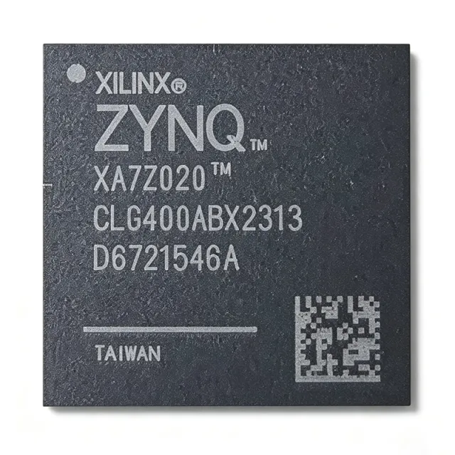
XC7Z020-2CLG484I - Zynq-7000 SoC 85K Logic Cells | AMD
MPN: XC7Z020-2CLG484I ✓ Active| Qty | Unit Price | Extended |
|---|---|---|
| 1 | $60.07 | $60.07 |
| 10 | $57.1 | $571.00 |
| 100 | $54.2 | $5,420.00 |
| 500 | $51.5 | $25,750.00 |
| 1,000 | $49 | $49,000.00 |
XC7Z020-2CLG484I Overview
A System on Chip (SoC) is an integrated circuit that consolidates processor, memory controllers, peripherals, and programmable hardware on a single substrate. The Zynq-7000 family pairs an ARM-based processing system (PS) with programmable logic (PL) over high-bandwidth AXI interfaces, reducing board space, power, and system complexity versus discrete processor-plus-FPGA solutions.
Key features include a DDR3/DDR3L memory controller with ECC, USB 2.0, Gigabit Ethernet, and support for I/O voltages of 1.2V, 1.5V, 1.8V, 2.5V, and 3.3V. The -2 speed grade supports up to 766 MHz PS operation and 200 MHz+ fabric clocking. The industrial temperature grade (-40C to +100C) targets harsh environments.
Architecturally, the PS and PL are independent power domains with defined sequencing requirements (VCCINT, VCCAUX, VCCBRAM, VCCO). The device supports partial reconfiguration, allowing dynamic PL updates while the PS continues running. The memory controller delivers robust DDR3/DDR3L with ECC for industrial and automotive-class designs.
Typical applications include motor control, industrial automation, software-defined radio, video processing, and embedded vision. The device suits real-time processing with hardware acceleration, such as machine vision and high-speed data acquisition.
Design consideration: ensure correct power-rail sequencing and provide a configuration source (QSPI flash) and PS clock; refer to the Zynq-7000 TRM (UG585) for detailed guidance. Pricing from $60.07 (LCSC, as of 2026-08-29).
Drop-in alternatives for XC7Z020-2CLG484I — same package, pin-to-pin compatible. Different-package parts requiring PCB rework are excluded.
Variants in this series
Same-series models that are drop-in compatible with XC7Z020-2CLG484I (same form factor and footprint) — differing in Package, Family, Logic Cells, Mounting Type, Operating Temperature.
Quick Comparison Tool — Select alternative parts for side-by-side comparison:
XC7Z020-2CLG484C
✅ Drop-In📋 Reference alternative (not in catalog)
XC7Z020-1CLG484I
✅ Drop-In✓ In Stock
$45.9375 / Unit
View Datasheet →XC7Z030-2CLG484I
✅ Drop-In📋 Reference alternative (not in catalog)
XC7Z010-2CLG484I
✅ Drop-In ⚠️ Specs Unverified📋 Reference alternative (not in catalog)
XC7Z020-2CLG484I-ES
⚡ Same Package ⚠️ Specs Unverified📋 Reference alternative (not in catalog)
XC7Z020-2CLG484I Maximum Ratings & Electrical Characteristics
| Processor Core | Dual ARM Cortex-A9 MPCore with CoreSight |
| Maximum Processor Frequency | 766 MHz |
| FPGA Family | Zynq-7000 (Artix-7 class fabric) |
| Logic Cells | 85,000 |
| Look-Up Tables (LUTs) | 53,200 |
| Flip-Flops | 106,400 |
| DSP Slices | 220 |
| Block RAM | 4.9 Mb |
| User I/O | 140 (CLG484) |
| Speed Grade | -2 |
| Memory Controller | DDR3/DDR3L with ECC |
| Peripherals | USB 2.0, Gigabit Ethernet |
| I/O Voltages | 1.2V, 1.5V, 1.8V, 2.5V, 3.3V |
| Operating Temperature | -40C to +100C (Industrial) |
| Package | 484-CSPBGA (19x19 mm) |
| Mounting Type | Surface Mount |
XC7Z020-2CLG484I Pin Configuration
| Pin F17 | VCCINT — Core power supply (1.0V) |
| Pin AE20 | VCCAUX — Auxiliary power supply (1.8V) |
| Pin AC21 | VCCBRAM — Block RAM supply (1.0V) |
| Pin H4 | PS_DDR3 interface bank — PS DDR3/DDR3L memory controller I/O |
| Pin J15 | MIO — PS Multiplexed I/O for peripherals |
| Pin B24 | IO_Lx bank 34 — PL user I/O, bank 34 |
| Pin C2 | GND — Ground |
| Pin AB2 | PS_CLK — PS reference clock input (33.33 MHz typical) |
| Pin F9 | PS_POR_B — PS power-on reset |
| Pin AC24 | PS_MODE — Boot mode configuration pins |
Typical Applications
XC7Z020-2CLG484I is suitable for 6 applications: Industrial Motor Control, Software-Defined Radio, Embedded Vision Systems, Industrial Automation PLC, High-Speed Data Acquisition, Aerospace and Robotics Control.
Industrial Motor Control
The XC7Z020-2CLG484I fits motor control because its 220 DSP slices execute FOC (field-oriented control) math at high sampling rates while the dual Cortex-A9 at 766 MHz runs protocol stacks like EtherCAT. The industrial -40C to +100C rating matches factory environments, and 140 user I/O supports multi-axis encoder and PWM interfaces on one chip.
Recommended
Software-Defined Radio
SDR designs benefit from the device's 220 DSP slices for FIR filters and FFTs, and 4.9 Mb block RAM for buffering wideband streams. The high-bandwidth PS-to-PL AXI interfaces let the ARM cores handle MAC-layer processing while the fabric performs real-time DSP, achieving deterministic latency unattainable with software-only processors.
Recommended
Embedded Vision Systems
Machine vision pipelines use the FPGA fabric for ISP functions such as debayering, HDR merge, and lens correction at line rates, while the Cortex-A9 subsystem runs application logic and network streaming. The DDR3/DDR3L controller with ECC sustains the memory bandwidth required for multi-megapixel frame buffering in industrial cameras.
Recommended
Industrial Automation PLC
As a PLC main processor, the XC7Z020-2CLG484I combines deterministic FPGA-based I/O scanning with ARM-based ladder/IEC 61131-3 execution. Gigabit Ethernet and USB 2.0 provide fieldbus and commissioning interfaces, and the industrial temperature grade plus ECC memory controller deliver the reliability expected in 24/7 automation equipment.
Recommended
High-Speed Data Acquisition
The fabric captures data from high-speed ADCs over LVDS/DDR interfaces at rates beyond what a standalone MCU can handle, using 4.9 Mb block RAM as elastic buffers and DSP slices for on-the-fly digital down-conversion. The PS then packages results for Gigabit Ethernet streaming, making a single-chip DAQ head possible.
Recommended
Aerospace and Robotics Control
Robotics controllers exploit the Zynq architecture for sensor fusion: fabric-implemented encoders, PWM, and safety interlocks run deterministically while the ARM cores run ROS-style control loops. Partial reconfiguration allows in-field updates to the control fabric without interrupting the running processor subsystem.
Recommended
Recommended Products Summary
Engineering reference data for XC7Z020-2CLG484I — comparison, design guidance, and compliance information.
Selection Guide
Comparison with Alternatives
| Parameter | This Product | XC7Z020-2CLG484C | XC7Z020-1CLG484I | XC7Z030-2CLG484I | XC7Z010-2CLG484I |
|---|---|---|---|---|---|
| Package | 484-CSPBGA (19x19) | 484-CSPBGA - same | 484-CSPBGA - same | 484-CSPBGA - same | 484-CSPBGA - same |
| Brand | AMD (Xilinx) | AMD | AMD | AMD | AMD |
| Logic Cells | 85,000 | 85,000 | 85,000 | 125,000 | 43,000 |
| DSP Slices | 220 | 220 | 220 | 400 | 120 |
| Block RAM | 4.9 Mb | 4.9 Mb | 4.9 Mb | 6.6 Mb | 2.1 Mb |
| Max ARM Frequency | 766 MHz | 766 MHz | 667 MHz | 766 MHz | 766 MHz |
| Temperature Range | -40C to +100C (I) | 0C to +85C (C) | -40C to +100C (I) | -40C to +100C (I) | -40C to +100C (I) |
Key Differentiators
- Best price/performance balance in Zynq-7000 CLG484 family (vs XC7Z030-2CLG484I)
- Industrial temperature rating (vs XC7Z020-2CLG484C)
- Higher performance than cost-down variant (vs XC7Z010-2CLG484I)
Design Notes
The XC7Z020-2CLG484I uses multiple rails (VCCINT 1.0V, VCCAUX 1.8V, VCCBRAM 1.0V, per-bank VCCO). Follow the sequencing order in UG585 to prevent latch-up; use a PMBus sequencing PMIC or sequencer IC. Size VCCINT for full-logic utilization: 85K cells fully utilized can draw several amps of core current depending on clock rate and toggle activity - run Xilinx Power Estimator (XPE) early.
The 484-CSPBGA (19x19 mm, 1.0 mm pitch) typically requires 6+ layer PCBs with signal layers for DDR3 escape. Follow the HDK layout guidelines: length-match DDR3 byte lanes, keep 33.33 MHz PS_CLK away from switching rails, and provide dense via farms under the package for thermal and power delivery. Use X-ray inspection qualification if using standard soldering for BGA assembly.
At high fabric utilization with 766 MHz PS operation, junction temperature can approach the +100C industrial limit. Estimate dissipation with XPE, then size a heatsink or airflow; CLG484 theta_JA on multilayer boards is roughly [DATA_NEEDED: theta_JA value]. Monitor PS temperature via the XADC and implement firmware throttling for enclosed industrial products.
Two frequent mistakes: (1) omitting the configuration source - the SRAM fabric is volatile and needs QSPI/NAND/SD boot at every power cycle, so always design in QSPI flash and JTAG header; (2) boot mode strap errors on PS_MODE pins causing fallback boot. Verify mode pins with a scope at reset and validate with the Zynq TRM (UG585) boot flow.
Compliance Information
RoHS compliant per distributor listings. Verify REACH and conflict minerals status via AMD product compliance documentation.







