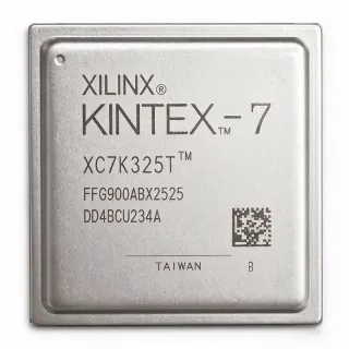
XC7K420T-2FFG901I - Kintex-7 FPGA, 416K Logic Cells | AMD
MPN: XC7K420T-2FFG901I ✓ Active| Qty | Unit Price | Extended |
|---|---|---|
| 1 | $6182.01 | $6,182.01 |
| 10 | $5800 | $58,000.00 |
| 100 | $5500 | $550,000.00 |
| 500 | $5200 | $2,600,000.00 |
| 1,000 | $4900 | $4,900,000.00 |
XC7K420T-2FFG901I Overview
A Field Programmable Gate Array (FPGA) is an integrated circuit that can be configured by the customer after manufacturing to implement any digital logic function. FPGAs sit within the broader hierarchy of programmable logic devices (PLDs), which are semiconductor components that allow hardware designers to implement custom digital circuits without the high non-recurring engineering costs of ASICs. Within this hierarchy, the Kintex-7 family is positioned as AMD's mid-range, price-performance optimized FPGA line, sitting between the low-power Artix-7 and the high-performance Virtex-7 families.
Key features of the XC7K420T-2FFG901I include 416,960 logic cells, 380 user I/Os, 30,744,140 bits of block RAM, and 1,680 DSP slices. The device operates from a 1V core supply and is built on a 28nm high-k metal gate (HKMG) process technology. The -2 speed grade provides a balanced performance point, and the I-grade temperature range supports operation from -40°C to +100°C (Tj).
The Kintex-7 architecture integrates 16 high-speed serial transceivers (GTX) capable of up to 12.5 Gb/s, along with hardened memory controllers, PCIe blocks, and mixed-mode clock managers (MMCMs) and PLLs. This integration enables the device to serve as a complete system-on-chip solution for high-bandwidth data path applications.
Typical applications include high-performance computing, wired and wireless communications, broadcast video, and aerospace and defense systems. The device's combination of logic density, DSP capability, and transceiver speed makes it suitable for software-defined radio, radar signal processing, and high-speed data acquisition.
When designing with this device, careful attention must be paid to power supply decoupling and thermal management. The 900-ball FCBGA package requires a robust PCB layout with multiple ground and power planes, and the core voltage must be regulated to 1.0V ±3% to ensure reliable operation.
Drop-in alternatives for XC7K420T-2FFG901I — same package, pin-to-pin compatible. Different-package parts requiring PCB rework are excluded.
Variants in this series
Same-series models that are drop-in compatible with XC7K420T-2FFG901I (same form factor and footprint) — differing in Block RAM, Logic Cells, Number of Pins, Operating Temperature.
Quick Comparison Tool — Select alternative parts for side-by-side comparison:
XC7K420T-1FFG901I
✅ Drop-In📋 Reference alternative (not in catalog)
XC7K480T-2FFG901I
✅ Drop-In✓ In Stock
$1095 / Unit
View Datasheet →XC7K420T-2FFG901I Maximum Ratings & Electrical Characteristics
| Family | Kintex-7 |
| Logic Cells | 416960 |
| Block RAM | 30781440 bits |
| DSP Slices | 1680 |
| User I/Os | 380 |
| Number of Inputs | 350 |
| Package | 900-BBGA, FCBGA |
| Number of Pins | 901 |
| Core Supply Voltage | 1V |
| Supply Voltage Range | 0.97V ~ 1.03V |
| Technology | 28nm |
| Speed Grade | -2 |
| Operating Temperature | -40C to +100C (Tj) |
| Mounting Type | Surface Mount |
| RoHS Status | Compliant |
XC7K420T-2FFG901I Pin Configuration
| Pin A1 | GND — Ground |
| Pin A2 | IO_L1P_T0_100 — User I/O bank 100 |
| Pin A3 | IO_L1N_T0_100 — User I/O bank 100 |
| Pin B1 | VCCINT — Internal core supply 1.0V |
| Pin B2 | IO_L2P_T0_100 — User I/O bank 100 |
| Pin B3 | IO_L2N_T0_100 — User I/O bank 100 |
| Pin C1 | GND — Ground |
| Pin C2 | IO_L3P_T0_100 — User I/O bank 100 |
| Pin C3 | IO_L3N_T0_100 — User I/O bank 100 |
| Pin D1 | VCCAUX — Auxiliary supply 1.8V |
| Pin D2 | IO_L4P_T0_100 — User I/O bank 100 |
| Pin D3 | IO_L4N_T0_100 — User I/O bank 100 |
Typical Applications
XC7K420T-2FFG901I is suitable for 6 applications: High-Performance Computing, Wired and Wireless Communications, Broadcast Video, Aerospace and Defense, Medical Imaging, Test and Measurement.
High-Performance Computing
The XC7K420T-2FFG901I is ideal for high-performance computing (HPC) applications such as data center acceleration and scientific computing. Its 416,960 logic cells and 1,680 DSP slices provide substantial parallel processing capability for workloads like financial modeling, genomics, and machine learning inference. The 28nm process and 1V core voltage enable high clock speeds while managing power dissipation. The device's high-speed serial transceivers (up to 12.5 Gb/s) facilitate fast data movement between FPGAs and host processors, making it suitable for PCIe-based accelerator cards. Designers can leverage the hardened memory controllers to interface with DDR3/DDR4 memory, ensuring high-bandwidth data access for compute-intensive tasks.
Recommended
Wired and Wireless Communications
In wired and wireless communications, the XC7K420T-2FFG901I excels in baseband processing, software-defined radio (SDR), and network infrastructure. Its 16 GTX transceivers support data rates up to 12.5 Gb/s, enabling high-speed serial links for CPRI, JESD204B, and 10GbE interfaces. The device's DSP slices are well-suited for digital up/down conversion, filtering, and FEC algorithms. The 380 user I/Os provide ample connectivity for ADCs, DACs, and PHY devices. The -2 speed grade ensures timing closure for high-throughput signal processing chains. Designers can implement complex modulation schemes and MIMO processing, making it a versatile choice for 5G, LTE, and radar systems.
Recommended
Broadcast Video
The XC7K420T-2FFG901I is well-suited for broadcast video applications, including video processing, format conversion, and image enhancement. Its high logic density supports complex video algorithms such as 4K/8K upscaling, frame rate conversion, and HDR processing. The device's block RAM (30.7 Mb) provides ample storage for line buffers and frame stores, while the DSP slices handle color space conversion and filtering. The 380 user I/Os can interface with SDI, HDMI, and DisplayPort PHYs. The 28nm process enables low power consumption, which is critical for broadcast equipment that operates 24/7. The device's reliability and long-term availability make it a trusted choice for professional video infrastructure.
Recommended
Aerospace and Defense
In aerospace and defense, the XC7K420T-2FFG901I is used in radar, electronic warfare, and secure communications systems. Its high DSP throughput and logic density enable real-time signal processing for pulse compression, beamforming, and target detection. The device's I-grade temperature range (-40°C to +100°C) ensures operation in harsh environments. The 28nm process provides a balance of performance and power, which is important for airborne and space-borne systems. The device's security features, including bitstream encryption, protect against unauthorized copying and tampering. The 900-ball FCBGA package offers excellent thermal performance, allowing reliable operation under high power dissipation.
Recommended
Medical Imaging
The XC7K420T-2FFG901I is well-suited for medical imaging systems such as CT scanners, MRI, and ultrasound. Its high logic density and DSP slices enable real-time image reconstruction, filtering, and enhancement. The device's block RAM supports large image buffers, while the high-speed transceivers facilitate data transfer from sensors and to display systems. The 28nm process ensures low power consumption, which is critical for portable and battery-powered devices. The device's reliability and long-term availability are essential for medical equipment that must meet stringent regulatory requirements. Designers can implement complex algorithms like beamforming and image fusion, making it a versatile choice for advanced medical imaging.
Recommended
Test and Measurement
The XC7K420T-2FFG901I is ideal for test and measurement equipment such as oscilloscopes, logic analyzers, and signal generators. Its high-speed transceivers and logic density enable real-time data acquisition, triggering, and analysis. The device's DSP slices handle waveform processing and FFT, while the block RAM supports deep memory buffers. The 380 user I/Os provide connectivity for high-speed ADCs and DACs. The -2 speed grade ensures high sample rates and low latency. The device's flexibility allows designers to implement custom triggering and measurement algorithms, making it a powerful platform for advanced test equipment.
Recommended
Recommended Products Summary
Engineering reference data for XC7K420T-2FFG901I — comparison, design guidance, and compliance information.
Selection Guide
Comparison with Alternatives
| Parameter | This Product | XC7K420T-1FFG901I | XC7K480T-2FFG901I | XC7K325T-2FFG676I | XC7K410T-2FFG900I |
|---|---|---|---|---|---|
| Package | 900-BBGA, FCBGA (901 pins) | 900-BBGA, FCBGA (901 pins) | 900-BBGA, FCBGA (901 pins) | 676-BBGA, FCBGA (676 pins) | 900-BBGA, FCBGA (900 pins) |
| Brand | AMD | AMD | AMD | AMD | AMD |
| Logic Cells | 416960 | 416960 | 477760 | 326080 | 406720 |
| Block RAM (bits) | 30781440 | 30781440 | 38338560 | 16025472 | 30317760 |
| DSP Slices | 1680 | 1680 | 1920 | 840 | 1540 |
| User I/Os | 380 | 380 | 380 | 400 | 400 |
| Speed Grade | -2 | -1 | -2 | -2 | -2 |
| Core Supply Voltage | 1V | 1V | 1V | 1V | 1V |
Key Differentiators
- Higher logic density than XC7K325T (vs XC7K325T-2FFG676I)
- More DSP slices than XC7K410T (vs XC7K410T-2FFG900I)
- Faster speed grade than XC7K420T-1FFG901I (vs XC7K420T-1FFG901I)
Design Notes
The XC7K420T-2FFG901I requires a 1.0V core supply (VCCINT) with tight regulation (±3%). Use a dedicated switching regulator with a low-noise LDO for the analog supplies (VCCAUX, VCCBRAM). Decouple each power pin with a 100nF ceramic capacitor and add bulk capacitance (10uF) per power rail. Follow AMD's power distribution network (PDN) guidelines to minimize voltage droop during high-speed switching.
The 900-ball FCBGA package can dissipate significant power, especially with high logic utilization and transceiver activity. Use a heatsink or active cooling for designs exceeding 10W. Ensure adequate airflow and consider the thermal resistance (theta_JA) of the package. The I-grade temperature range is -40°C to +100°C (Tj), so monitor junction temperature to avoid exceeding the maximum rating.
The 900-ball FCBGA requires a multi-layer PCB with dedicated power and ground planes. Use microvias and blind/buried vias for signal routing to escape the dense ball grid. Follow AMD's PCB design guidelines for high-speed serial transceivers, including controlled impedance traces and proper ground referencing. Place decoupling capacitors close to the power pins to minimize parasitic inductance.
Compliance Information
RoHS compliant per JLCPCB listing. AEC-Q100 not applicable for FPGA. Other compliance data not specified in provided sources.