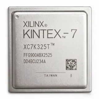
XC7K480T-2FFG901I - Kintex-7 FPGA 477K Logic Cells | AMD
MPN: XC7K480T-2FFG901I ✓ Active| Qty | Unit Price | Extended |
|---|---|---|
| 1 | $1495 | $1,495.00 |
| 10 | $1395 | $13,950.00 |
| 100 | $1295 | $129,500.00 |
| 500 | $1195 | $597,500.00 |
| 1,000 | $1095 | $1,095,000.00 |
XC7K480T-2FFG901I Overview
A Field Programmable Gate Array (FPGA) is an integrated circuit that can be configured by the customer after manufacturing to implement any digital logic function. FPGAs sit within the hierarchy of programmable logic devices, offering more capacity and flexibility than CPLDs, and are used as an alternative to ASICs for prototyping, low-to-mid volume production, and applications requiring field-updatable hardware. The Kintex-7 family balances cost, power, and performance, making it a popular choice for a wide range of systems.
Key features of the XC7K480T-2FFG901I include 477,760 logic cells, 35,205,120 bits of block RAM, and 380 user I/Os. It operates at a core voltage of 1V and is available in a 900-pin FCBGA package. The device supports multiple I/O standards, high-speed transceivers, and includes hardened memory controllers and DSP slices for signal processing. The -2 speed grade offers a balance of performance and power.
Technically, the Kintex-7 family uses a unified architecture with configurable logic blocks (CLBs), block RAM, DSP48E1 slices, and clock management tiles (CMTs) with MMCM and PLL. The 28nm high-k metal gate (HKMG) process technology enables high performance with lower power compared to previous generations. The device supports partial reconfiguration and advanced clocking, making it suitable for complex, high-bandwidth systems.
Typical applications include high-performance computing, wired and wireless communications, aerospace and defense, broadcast, and medical imaging. The high logic density and DSP capability make it ideal for signal processing, packet processing, and video processing. The 380 I/Os and high-speed transceivers enable connectivity to various peripherals and backplanes.
When designing with this device, careful attention must be paid to power supply decoupling, thermal management, and signal integrity. The FCBGA package requires a multi-layer PCB with proper via placement and ground planes. Use the AMD Vivado design suite for configuration and implementation.
Drop-in alternatives for XC7K480T-2FFG901I — same package, pin-to-pin compatible. Different-package parts requiring PCB rework are excluded.
Variants in this series
Same-series models that are drop-in compatible with XC7K480T-2FFG901I (same form factor and footprint) — differing in Operating Temperature, Block RAM, Logic Cells, Speed Grade, Number of Pins.
Quick Comparison Tool — Select alternative parts for side-by-side comparison:
XC7K480T-2FFG901C
✅ Drop-In ⚠️ Specs Unverified📋 Reference alternative (not in catalog)
XC7K480T-3FFG901I
✅ Drop-In ⚠️ Specs Unverified📋 Reference alternative (not in catalog)
XC7K480T-1FFG901I
✅ Drop-In ⚠️ Specs Unverified✓ In Stock
$5200 / Unit
View Datasheet →XC7K480T-2FFG900I
✅ Drop-In ⚠️ Specs Unverified📋 Reference alternative (not in catalog)
XC7K480T-2FFG901C
✅ Drop-In ⚠️ Specs Unverified📋 Reference alternative (not in catalog)
XC7K480T-2FFG901I Maximum Ratings & Electrical Characteristics
| Family | Kintex-7 |
| Logic Cells | 477760 |
| Block RAM | 35205120 bits |
| Number of I/Os | 380 |
| Package | 900-BBGA, FCBGA |
| Technology | 28nm |
| Core Voltage | 1V |
| Speed Grade | -2 |
| Operating Temperature | Industrial (-40C to +100C) |
| Mounting Type | Surface Mount |
| Number of Pins | 900 |
| RoHS Status | Compliant |
| Supply Voltage | 1V |
XC7K480T-2FFG901I Pin Configuration
| Pin A1 | IO_L1P_T0 — User I/O bank 0 |
| Pin A2 | IO_L1N_T0 — User I/O bank 0 |
| Pin B1 | IO_L2P_T0 — User I/O bank 0 |
| Pin B2 | IO_L2N_T0 — User I/O bank 0 |
| Pin C1 | VCC — Core supply voltage 1V |
| Pin C2 | GND — Ground |
| Pin D1 | IO_L3P_T0 — User I/O bank 0 |
| Pin D2 | IO_L3N_T0 — User I/O bank 0 |
| Pin E1 | IO_L4P_T0 — User I/O bank 0 |
| Pin E2 | IO_L4N_T0 — User I/O bank 0 |
| Pin F1 | VCC — Core supply voltage 1V |
| Pin F2 | GND — Ground |
Typical Applications
XC7K480T-2FFG901I is suitable for 6 applications: High-Performance Computing, Wired and Wireless Communications, Aerospace and Defense, Broadcast and Video Processing, Medical Imaging, Test and Measurement.
High-Performance Computing
The XC7K480T-2FFG901I provides 477,760 logic cells and 35,205,120 block RAM bits, making it ideal for high-performance computing tasks such as data acceleration, AI inference, and complex algorithm implementation. The 380 I/Os and high-speed transceivers enable high-bandwidth data movement between processing elements and memory. The 28nm process balances performance and power, allowing for dense logic integration in a single device. This FPGA can be used to accelerate workloads in data centers, scientific computing, and financial modeling, where parallel processing and low latency are critical. The large logic capacity supports custom datapaths and pipelined architectures, while the block RAM provides on-chip storage for intermediate results, reducing external memory traffic and improving overall system throughput.
Recommended
Wired and Wireless Communications
The XC7K480T-2FFG901I is well-suited for wired and wireless communication systems, including base stations, routers, and switches. Its high logic density and DSP capabilities enable efficient implementation of signal processing algorithms, such as FFT, filtering, and modulation/demodulation. The 380 I/Os support various high-speed interfaces, while the high-speed transceivers handle serial data links. The 28nm technology provides a good balance of performance and power, making it suitable for power-sensitive communication equipment. The device can be configured to support multiple protocols, including Ethernet, CPRI, and JESD204B, allowing for flexible system design. The large block RAM can be used for packet buffering and queue management, essential for high-throughput networking applications.
Recommended
Aerospace and Defense
The XC7K480T-2FFG901I is designed for aerospace and defense applications, offering high reliability and performance in harsh environments. The industrial temperature grade (-40C to +100C) ensures operation in extreme conditions. The 477,760 logic cells and 35,205,120 block RAM bits provide ample resources for radar, sonar, and electronic warfare systems. The 380 I/Os support various sensor interfaces, while the high-speed transceivers enable data links to other systems. The 28nm process offers a good balance of performance and power, critical for power-constrained platforms. The device can be used for real-time signal processing, image processing, and secure communications. Its reconfigurability allows for field updates and adaptation to changing mission requirements.
Recommended
Broadcast and Video Processing
The XC7K480T-2FFG901I is ideal for broadcast and video processing applications, including video switchers, encoders, and decoders. Its high logic density and DSP capabilities enable efficient implementation of video codecs, scaling, and color space conversion. The 380 I/Os support various video interfaces, such as SDI, HDMI, and DisplayPort. The 28nm technology provides the performance needed for real-time 4K and 8K video processing. The large block RAM can be used for line buffers and frame storage, essential for video processing pipelines. The device can be configured to handle multiple video streams simultaneously, making it suitable for broadcast infrastructure. Its reconfigurability allows for support of evolving video standards and formats.
Recommended
Medical Imaging
The XC7K480T-2FFG901I is well-suited for medical imaging systems, such as CT scanners, MRI, and ultrasound. Its high logic density and DSP capabilities enable efficient implementation of image reconstruction, filtering, and enhancement algorithms. The 380 I/Os support various sensor interfaces, while the high-speed transceivers enable data transfer to host systems. The 28nm process offers a good balance of performance and power, critical for medical equipment. The device can be used for real-time image processing, enabling faster diagnosis and improved image quality. The large block RAM can be used for image storage and processing pipelines. Its reconfigurability allows for algorithm updates and customization for specific imaging modalities.
Recommended
Test and Measurement
The XC7K480T-2FFG901I is ideal for test and measurement equipment, including oscilloscopes, logic analyzers, and signal generators. Its high logic density and DSP capabilities enable efficient implementation of data acquisition, triggering, and signal analysis. The 380 I/Os support various probe interfaces, while the high-speed transceivers enable high-bandwidth data capture. The 28nm technology provides the performance needed for high-speed signal processing. The large block RAM can be used for data buffering and waveform storage. The device can be configured to support multiple measurement modes and protocols, making it versatile for various test applications. Its reconfigurability allows for firmware updates and feature enhancements.
Recommended
Recommended Products Summary
Engineering reference data for XC7K480T-2FFG901I — comparison, design guidance, and compliance information.
Selection Guide
Comparison with Alternatives
| Parameter | This Product | XC7K480T-2FFG901C | XC7K480T-3FFG901I | XC7K480T-1FFG901I | XC7K480T-2FFG900I |
|---|---|---|---|---|---|
| Package | 900-BBGA, FCBGA | 900-BBGA, FCBGA | 900-BBGA, FCBGA | 900-BBGA, FCBGA | 900-BBGA, FCBGA |
| Brand | AMD | AMD | AMD | AMD | AMD |
| Logic Cells | 477760 | 477760 | 477760 | 477760 | 477760 |
| Block RAM | 35205120 bits | 35205120 bits | 35205120 bits | 35205120 bits | 35205120 bits |
| Number of I/Os | 380 | 380 | 380 | 380 | 380 |
| Speed Grade | -2 | -2 | -3 | -1 | -2 |
| Temperature Grade | Industrial (-40C to +100C) | Commercial (0C to +85C) | Industrial (-40C to +100C) | Industrial (-40C to +100C) | Industrial (-40C to +100C) |
| Core Voltage | 1V | 1V | 1V | 1V | 1V |
Key Differentiators
- Industrial temperature grade (vs XC7K480T-2FFG901C)
- Balanced -2 speed grade (vs XC7K480T-1FFG901I)
- High logic density (vs XC7K325T-2FFG900I)
Design Notes
The XC7K480T-2FFG901I requires a stable 1V core supply. Use a dedicated power management IC with sufficient current capability. Decouple each power pin with a 100nF ceramic capacitor and add bulk capacitance (10uF or more) near the FPGA. Follow the power supply sequencing requirements in the datasheet to avoid damage.
The XC7K480T-2FFG901I can dissipate significant power, especially at high utilization. Use a heatsink and ensure adequate airflow. The FCBGA package has a thermal pad that must be soldered to a thermal via array on the PCB. Monitor junction temperature and keep it below the maximum rating. Consider using a thermal simulation tool during design.
The 900-ball FCBGA package requires a multi-layer PCB with at least 8-10 layers. Use controlled impedance traces for high-speed signals. Place decoupling capacitors close to the FPGA power pins. Ensure proper ground plane continuity. Follow the layout guidelines in UG475 for pinout and routing.
Compliance Information
RoHS compliant per distributor data. AEC-Q100 not applicable for FPGA.