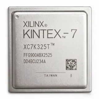
XC7K355T-2FFG901I - Kintex-7 FPGA 356K Logic Cells | AMD
MPN: XC7K355T-2FFG901I ✓ Active| Qty | Unit Price | Extended |
|---|---|---|
| 1 | $1250 | $1,250.00 |
| 10 | $1180 | $11,800.00 |
| 100 | $1100 | $110,000.00 |
| 500 | $1050 | $525,000.00 |
| 1,000 | $990 | $990,000.00 |
XC7K355T-2FFG901I Overview
An FPGA (Field Programmable Gate Array) is an integrated circuit that can be configured by the customer or designer after manufacturing. Unlike fixed-function ASICs, FPGAs contain an array of programmable logic blocks and reconfigurable interconnects, allowing for rapid prototyping and flexible hardware design. The Kintex-7 family is positioned as a mid-to-high-range solution, providing substantial logic density, advanced DSP capabilities, and high-speed serial connectivity.
Key features of the XC7K355T-2FFG901I include 27,825 CLBs, 710 DSP slices, and support for MMCM and PLL clock management. The device operates at a maximum frequency of 1286 MHz and is built on 28nm CMOS technology. The FCBGA-901 package offers excellent thermal and electrical performance, with a compact footprint suitable for space-constrained designs.
Technically, the Kintex-7 architecture integrates a flexible 6-input look-up table (LUT) fabric, dedicated block RAM, and high-speed transceivers. The device supports various configuration methods including JTAG, master SPI, and slave SelectMAP. Its advanced power management features enable efficient operation across different performance modes.
Typical applications include software-defined radio, high-performance computing, medical imaging, and video processing. The XC7K355T's combination of logic density and DSP capability makes it ideal for signal processing tasks that require parallel computation.
When designing with this FPGA, ensure adequate decoupling capacitors on all power rails and follow the recommended power-up sequence to avoid latch-up. The device requires careful thermal management due to its high power dissipation at full utilization.
Drop-in alternatives for XC7K355T-2FFG901I — same package, pin-to-pin compatible. Different-package parts requiring PCB rework are excluded.
Variants in this series
Same-series models that are drop-in compatible with XC7K355T-2FFG901I (same form factor and footprint) — differing in Mounting Type, Block RAM, Logic Cells, Temperature Grade, User I/O.
Quick Comparison Tool — Select alternative parts for side-by-side comparison:
XC7K410T-2FFG901I
✅ Drop-In📋 Reference alternative (not in catalog)
XC7K325T-2FFG900I
✅ Drop-In ⚠️ Specs Unverified✓ In Stock
$65 / Unit
View Datasheet →XC7K355T-1FFG901I
✅ Drop-In ⚠️ Specs Unverified✓ In Stock
Contact for price
XC7K355T-2FFG901C
✅ Drop-In ⚠️ Specs Unverified📋 Reference alternative (not in catalog)
XC7K355T-3FFG901I
✅ Drop-In ⚠️ Specs Unverified📋 Reference alternative (not in catalog)
XC7K355T-2FFG901I Maximum Ratings & Electrical Characteristics
| Family | Kintex-7 |
| Number of Logic Elements/Cells | 356160 |
| Number of LABs/CLBs | 27825 |
| Total RAM Bits | 26357760 |
| Number of I/O | 300 |
| Operating Supply Voltage | 0.97 V ~ 1.03 V |
| Operating Temperature Range | -40°C ~ 100°C (TJ) |
| Package | 900-BBGA, FCBGA |
| Mounting Type | SMD |
| Maximum Frequency | 1286 MHz |
| Technology | 28nm CMOS |
| Number of CLBs | 27825 |
| RoHS Status | Compliant |
XC7K355T-2FFG901I Pin Configuration
| Pin A1 | IO_L1P_T0 — User I/O bank 0 |
| Pin A2 | IO_L1N_T0 — User I/O bank 0 |
| Pin B1 | VCCINT — Internal core voltage 1.0V |
| Pin B2 | GND — Ground |
| Pin C1 | IO_L2P_T0 — User I/O bank 0 |
| Pin C2 | IO_L2N_T0 — User I/O bank 0 |
| Pin D1 | VCCAUX — Auxiliary voltage 1.8V |
| Pin D2 | GND — Ground |
| Pin E1 | IO_L3P_T0 — User I/O bank 0 |
| Pin E2 | IO_L3N_T0 — User I/O bank 0 |
| Pin F1 | VCCIO_0 — I/O bank 0 voltage |
| Pin F2 | GND — Ground |
Typical Applications
XC7K355T-2FFG901I is suitable for 6 applications: Software Defined Radio, High-Performance Computing, Medical Imaging, Video Processing, Aerospace and Defense, Industrial Automation.
Software Defined Radio
The XC7K355T-2FFG901I is ideal for software-defined radio (SDR) systems due to its high DSP capability and 300 I/Os. It can handle complex modulation schemes and multiple channels simultaneously. The 28nm technology ensures low power consumption, critical for portable and field-deployed SDR units. Its 356,160 logic cells provide ample resources for implementing digital down/up converters, filters, and protocol stacks.
Recommended
High-Performance Computing
In high-performance computing (HPC), the XC7K355T-2FFG901I accelerates data-intensive algorithms through massive parallelism. Its 356,160 logic cells and 26,357,760 RAM bits enable efficient implementation of custom arithmetic units and data pipelines. The device's 1286 MHz maximum frequency supports high-throughput processing. It is commonly used in financial modeling, scientific simulations, and big data analytics where low latency is crucial.
Recommended
Medical Imaging
The XC7K355T-2FFG901I excels in medical imaging applications like ultrasound and MRI. Its DSP slices and high logic density enable real-time image processing, including filtering, enhancement, and reconstruction. The 300 I/Os interface with high-speed ADCs and display controllers. The industrial temperature range (-40°C to 100°C) ensures reliable operation in clinical environments. Its low power consumption is beneficial for portable medical devices.
Recommended
Video Processing
For video processing, the XC7K355T-2FFG901I provides the parallel processing power needed for real-time 4K/8K video streams. Its 356,160 logic cells can implement multiple video codecs, scalers, and color space converters. The 26,357,760 RAM bits support large frame buffers. With 300 I/Os, it easily connects to HDMI, DisplayPort, and camera interfaces. The device's high bandwidth enables low-latency video analytics for surveillance and broadcasting.
Recommended
Aerospace and Defense
The XC7K355T-2FFG901I is suitable for aerospace and defense applications due to its industrial temperature range and high reliability. It is used in radar, electronic warfare, and secure communication systems. The 28nm technology provides radiation tolerance with proper mitigation. Its 300 I/Os interface with various sensors and actuators. The device's reconfigurability allows for in-field updates, essential for evolving mission requirements.
Recommended
Industrial Automation
In industrial automation, the XC7K355T-2FFG901I enables real-time control and monitoring of complex machinery. Its logic cells implement custom motor control algorithms, PLCs, and vision systems. The 300 I/Os connect to encoders, sensors, and actuators. The device's industrial temperature range ensures operation in harsh factory environments. Its low power consumption reduces heat generation, simplifying thermal management in control cabinets.
Recommended
Recommended Products Summary
Engineering reference data for XC7K355T-2FFG901I — comparison, design guidance, and compliance information.
Selection Guide
Comparison with Alternatives
| Parameter | This Product | XC7K410T-2FFG901I | XC7K325T-2FFG900I | XC7K355T-1FFG901I |
|---|---|---|---|---|
| Package | 900-BBGA, FCBGA | 900-BBGA, FCBGA - same | 900-BBGA, FCBGA - same | 900-BBGA, FCBGA - same |
| Brand | AMD | AMD | AMD | AMD |
| Logic Cells | 356160 | 406720 | 326080 | 356160 |
| RAM Bits | 26357760 | 28660800 | 16025472 | 26357760 |
| I/O Count | 300 | 300 | 300 | 300 |
| Speed Grade | -2 | -2 | -2 | -1 |
| Temperature Range | -40°C to 100°C | -40°C to 100°C | -40°C to 100°C | -40°C to 100°C |
| Supply Voltage | 0.97V to 1.03V | 0.97V to 1.03V | 0.97V to 1.03V | 0.97V to 1.03V |
Key Differentiators
- Higher logic density than XC7K325T (vs XC7K325T-2FFG900I)
- Lower cost than XC7K410T (vs XC7K410T-2FFG901I)
- Industrial temperature grade (vs XC7K355T-2FFG901C)
Design Notes
The XC7K355T-2FFG901I requires a 1.0V core supply (VCCINT) and 1.8V auxiliary supply (VCCAUX). Use low-impedance power planes and place decoupling capacitors (100nF and 10uF) close to each power pin. Follow the recommended power-up sequence: VCCINT, then VCCAUX, then VCCIO to avoid latch-up. Refer to AMD UG475 for detailed power supply design guidelines.
The FCBGA-901 package can dissipate significant heat at full utilization. Use a thermal analysis tool to estimate junction temperature. For high-power designs, consider adding a heatsink or forced air cooling. The maximum junction temperature is 100°C, so ensure adequate thermal management to maintain reliability. Use thermal vias under the package to improve heat transfer to the PCB.
For the FCBGA-901 package, use a high-layer-count PCB (at least 12 layers) to route all 300 I/Os and power. Maintain controlled impedance for high-speed signals. Place the FPGA close to memory devices to minimize trace lengths. Use via-in-pad for fine-pitch BGA connections. Follow AMD's PCB design guidelines in UG475 for optimal signal integrity.
Compliance Information
RoHS compliant per AMD product page. Not AEC-Q100 qualified as it is not an automotive-grade part.