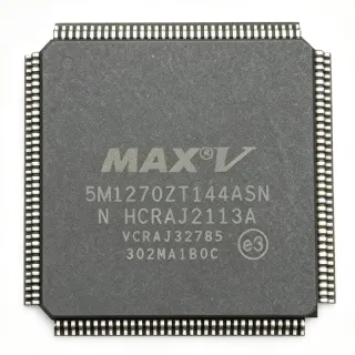
EPM570T144-5 - MAX II CPLD 570 LE, 144-pin TQFP | Altera
N.º da peça: EPM570T144-5 ✓ Ativo| Qtd. | Preço unitário | Total |
|---|---|---|
| 1 | $16.5 | $16,50 |
| 10 | $14.85 | $148,50 |
| 100 | $12.95 | $1.295,00 |
| 500 | $11.2 | $5.600,00 |
| 1.000 | $9.85 | $9.850,00 |
EPM570T144-5 Visão geral
A Complex Programmable Logic Device (CPLD) is a non-volatile, instant-on programmable logic device positioned hierarchically between discrete glue logic (74-series TTL/CMOS) and larger FPGAs. CPLDs deliver deterministic propagation delay, predictable pin-to-pin timing and battery-free configuration retention, making them ideal as interface bridges, address decoders, configuration controllers and machine-state controllers in systems built around microprocessors, microcontrollers or ASSPs. MAX II is Altera's lowest-cost CPLD family and the EPM570 sits at the top of that family's density ladder.
Key features of the EPM570T144-5 include 570 logic elements, 4 user I/O banks with MultiVolt I/O support (1.5 V, 1.8 V, 2.5 V, 3.3 V), a 116-user-I/O count in the TQFP-144 footprint, on-chip user Flash memory (UFM) block, an in-system programmability (ISP) interface via JTAG, and an internal oscillator. The "-5" speed grade offers a tPD1 of approximately 5.0 ns, supporting designs clocked above 100 MHz internally and 200 MHz via dedicated clock networks, while commercial and industrial temperature grades provide operating range flexibility.
Architecturally the EPM570 uses a non-volatile Flash configuration cell to retain the bitstream without external boot memory. The logic-array-blocks (LABs) are interconnected through a continuous MultiTrack interconnect, and routing is software-managed by the Quartus II / Quartus Prime toolchain. This architecture delivers instant-on operation: the device is functional within microseconds of power-up, eliminating the configuration-wait window typical of SRAM-based FPGAs.
Typical applications include 3.3 V / 2.5 V / 1.8 V bus interface bridging, glue logic for microprocessors (8051, ARM Cortex-M, PowerPC), I/O expansion for FPGAs and ASICs, address decoding and chip-select generation, LED driving, configuration watchdog and reset sequencing, and industrial control / portable / power-management designs where instant-on behaviour is essential.
When designing with the EPM570T144-5, ensure each VCCIO bank is decoupled with 0.1 µF and 10 µF capacitors placed close to the supply pins. The MultiVolt core allows the VCCINT supply to be powered at 3.3 V or 2.5 V while individual I/O banks interface to lower-voltage rails. JTAG programming pins (TCK, TMS, TDI, TDO) must be accessible for in-system updates; pull-ups on TCK, TMS and TDI are recommended per Altera's guidelines.
This page consolidates distributor stock and pricing for the EPM570T144-5, drop-in compatible alternatives from the same MAX II family and competitor CPLD lines, and practical design notes that go beyond the manufacturer datasheet.
Alternativas drop-in para EPM570T144-5 — mesmo encapsulamento, compatível pino a pino. Peças de encapsulamento diferente que exigem retrabalho na PCB são excluídas.
Variantes desta série
Modelos da mesma série compatíveis como drop-in com EPM570T144-5 (mesmo formato e footprint) — diferindo em Package, Programming Interface, Operating Temperature, Process Technology, Maximum User I/O Pins.
Ferramenta de comparação rápida — selecione peças alternativas para comparação lado a lado:
EPM570T144C5N
✅ Drop-In✓ Em estoque
$9.35 / unidade
Ver ficha técnica →EPM570T144C4N
✅ Drop-In✓ Em estoque
$25.1 / unidade
Ver ficha técnica →EPM570T144A5N
✅ Drop-In ⚠️ Especificações não verificadas✓ Em estoque
$22.8 / unidade
Ver ficha técnica →EPM570GT144C5N
✅ Drop-In✓ Em estoque
$14.2 / unidade
Ver ficha técnica →LC4256ZE-5TN144C
✅ Drop-In📋 Alternativa de referência (fora do catálogo)
LC4128ZE-5TN144C
✅ Drop-In📋 Alternativa de referência (fora do catálogo)
EPM570T144-5 Classificações máximas e características elétricas
| Family | MAX II |
| Device | EPM570 |
| Logic Elements (LE) | 570 |
| Macrocells (typical) | 440 |
| User I/O Pins | 116 |
| Encapsulamento | TQFP-144 (T144) |
| Contagem de pinos | 144 |
| Speed Grade | -5 (≈5.0 ns tPD1) |
| Process Technology | 0.18 µm |
| Non-volatile Configuration | Internal Flash (instant-on) |
| User Flash Memory (UFM) | 8 Kbits |
| I/O Banks | 4 |
| MultiVolt I/O Support | 1.5 V, 1.8 V, 2.5 V, 3.3 V |
| VCCINT | 3.3 V or 2.5 V (per bank group) |
| Programming Interface | JTAG (IEEE 1149.1 / IEEE 1532) |
| Status RoHS | Depends on date code (pre-2010 lots non-RoHS; lead-free Pb-free opt. available) |
Configuração de pinos do EPM570T144-5
| Pino 1 | I/O — General-purpose user I/O pin (Bank 1) |
| Pino 2 | I/O — General-purpose user I/O pin (Bank 1) |
| Pino 3 | I/O — General-purpose user I/O pin (Bank 1) |
| Pino 4 | I/O — General-purpose user I/O pin (Bank 1) |
| Pino 5 | I/O — General-purpose user I/O pin (Bank 1) |
| Pino 6 | I/O — General-purpose user I/O pin (Bank 1) |
| Pino 7 | VCCIO1 — Bank 1 I/O supply voltage (1.5/1.8/2.5/3.3 V) |
| Pino 8 | I/O — General-purpose user I/O pin (Bank 1) |
| Pino 9 | I/O — General-purpose user I/O pin (Bank 1) |
| Pino 10 | I/O — General-purpose user I/O pin (Bank 1) |
| Pino 11 | GND — Ground |
| Pino 12 | I/O — General-purpose user I/O pin (Bank 1) |
| Pino 13 | I/O — General-purpose user I/O pin (Bank 1) |
| Pino 14 | I/O — General-purpose user I/O pin (Bank 1) |
| Pino 15 | I/O — General-purpose user I/O pin (Bank 1) |
| Pino 16 | I/O — General-purpose user I/O pin (Bank 1) |
| Pino 17 | VCCINT — Core supply voltage (3.3 V or 2.5 V) |
| Pino 18 | I/O — General-purpose user I/O pin (Bank 2) |
| Pino 19 | I/O — General-purpose user I/O pin (Bank 2) |
| Pino 20 | I/O — General-purpose user I/O pin (Bank 2) |
| Pino 21 | GND — Ground |
| Pino 22 | I/O — General-purpose user I/O pin (Bank 2) |
| Pino 23 | I/O — General-purpose user I/O pin (Bank 2) |
| Pino 24 | I/O — General-purpose user I/O pin (Bank 2) |
| Pino 25 | I/O — General-purpose user I/O pin (Bank 2) |
| Pino 26 | I/O — General-purpose user I/O pin (Bank 2) |
| Pino 27 | VCCIO2 — Bank 2 I/O supply voltage (1.5/1.8/2.5/3.3 V) |
| Pino 28 | I/O — General-purpose user I/O pin (Bank 2) |
| Pino 29 | I/O — General-purpose user I/O pin (Bank 2) |
| Pino 30 | I/O — General-purpose user I/O pin (Bank 2) |
| Pino 31 | I/O — General-purpose user I/O pin (Bank 2) |
| Pino 32 | I/O — General-purpose user I/O pin (Bank 2) |
| Pino 33 | GND — Ground |
| Pino 34 | I/O — General-purpose user I/O pin (Bank 2) |
| Pino 35 | I/O — General-purpose user I/O pin (Bank 2) |
| Pino 36 | I/O — General-purpose user I/O pin (Bank 2) |
| Pino 37 | I/O — General-purpose user I/O pin (Bank 2) |
| Pino 38 | I/O — General-purpose user I/O pin (Bank 2) |
| Pino 39 | I/O — General-purpose user I/O pin (Bank 2) |
| Pino 40 | I/O — General-purpose user I/O pin (Bank 2) |
| Pino 41 | VCCINT — Core supply voltage (3.3 V or 2.5 V) |
| Pino 42 | I/O — General-purpose user I/O pin (Bank 2) |
| Pino 43 | I/O — General-purpose user I/O pin (Bank 2) |
| Pino 44 | I/O — General-purpose user I/O pin (Bank 2) |
| Pino 45 | GND — Ground |
| Pino 46 | I/O — General-purpose user I/O pin (Bank 2) |
| Pino 47 | I/O — General-purpose user I/O pin (Bank 2) |
| Pino 48 | I/O — General-purpose user I/O pin (Bank 2) |
| Pino 49 | I/O — General-purpose user I/O pin (Bank 2) |
| Pino 50 | I/O — General-purpose user I/O pin (Bank 2) |
| Pino 51 | VCCIO2 — Bank 2 I/O supply voltage (1.5/1.8/2.5/3.3 V) |
| Pino 52 | I/O — General-purpose user I/O pin (Bank 2) |
| Pino 53 | I/O — General-purpose user I/O pin (Bank 2) |
| Pino 54 | I/O — General-purpose user I/O pin (Bank 2) |
| Pino 55 | I/O — General-purpose user I/O pin (Bank 2) |
| Pino 56 | I/O — General-purpose user I/O pin (Bank 2) |
| Pino 57 | GND — Ground |
| Pino 58 | I/O — General-purpose user I/O pin (Bank 2) |
| Pino 59 | I/O — General-purpose user I/O pin (Bank 2) |
| Pino 60 | I/O — General-purpose user I/O pin (Bank 2) |
| Pino 61 | I/O — General-purpose user I/O pin (Bank 2) |
| Pino 62 | I/O — General-purpose user I/O pin (Bank 2) |
| Pino 63 | I/O — General-purpose user I/O pin (Bank 2) |
| Pino 64 | I/O — General-purpose user I/O pin (Bank 2) |
| Pino 65 | VCCINT — Core supply voltage (3.3 V or 2.5 V) |
| Pino 66 | I/O — General-purpose user I/O pin (Bank 2) |
| Pino 67 | I/O — General-purpose user I/O pin (Bank 2) |
| Pino 68 | I/O — General-purpose user I/O pin (Bank 2) |
| Pino 69 | GND — Ground |
| Pino 70 | I/O — General-purpose user I/O pin (Bank 3) |
| Pino 71 | I/O — General-purpose user I/O pin (Bank 3) |
| Pino 72 | I/O — General-purpose user I/O pin (Bank 3) |
| Pino 73 | I/O — General-purpose user I/O pin (Bank 3) |
| Pino 74 | I/O — General-purpose user I/O pin (Bank 3) |
| Pino 75 | VCCIO3 — Bank 3 I/O supply voltage (1.5/1.8/2.5/3.3 V) |
| Pino 76 | I/O — General-purpose user I/O pin (Bank 3) |
| Pino 77 | I/O — General-purpose user I/O pin (Bank 3) |
| Pino 78 | I/O — General-purpose user I/O pin (Bank 3) |
| Pino 79 | I/O — General-purpose user I/O pin (Bank 3) |
| Pino 80 | I/O — General-purpose user I/O pin (Bank 3) |
| Pino 81 | GND — Ground |
| Pino 82 | I/O — General-purpose user I/O pin (Bank 3) |
| Pino 83 | I/O — General-purpose user I/O pin (Bank 3) |
| Pino 84 | I/O — General-purpose user I/O pin (Bank 3) |
| Pino 85 | I/O — General-purpose user I/O pin (Bank 3) |
| Pino 86 | I/O — General-purpose user I/O pin (Bank 3) |
| Pino 87 | I/O — General-purpose user I/O pin (Bank 3) |
| Pino 88 | I/O — General-purpose user I/O pin (Bank 3) |
| Pino 89 | VCCINT — Core supply voltage (3.3 V or 2.5 V) |
| Pino 90 | I/O — General-purpose user I/O pin (Bank 3) |
| Pino 91 | I/O — General-purpose user I/O pin (Bank 3) |
| Pino 92 | I/O — General-purpose user I/O pin (Bank 3) |
| Pino 93 | GND — Ground |
| Pino 94 | I/O — General-purpose user I/O pin (Bank 3) |
| Pino 95 | I/O — General-purpose user I/O pin (Bank 3) |
| Pino 96 | I/O — General-purpose user I/O pin (Bank 3) |
| Pino 97 | I/O — General-purpose user I/O pin (Bank 3) |
| Pino 98 | I/O — General-purpose user I/O pin (Bank 3) |
| Pino 99 | VCCIO3 — Bank 3 I/O supply voltage (1.5/1.8/2.5/3.3 V) |
| Pino 100 | I/O — General-purpose user I/O pin (Bank 3) |
| Pino 101 | I/O — General-purpose user I/O pin (Bank 3) |
| Pino 102 | I/O — General-purpose user I/O pin (Bank 3) |
| Pino 103 | I/O — General-purpose user I/O pin (Bank 3) |
| Pino 104 | I/O — General-purpose user I/O pin (Bank 3) |
| Pino 105 | GND — Ground |
| Pino 106 | I/O — General-purpose user I/O pin (Bank 4) |
| Pino 107 | I/O — General-purpose user I/O pin (Bank 4) |
| Pino 108 | I/O — General-purpose user I/O pin (Bank 4) |
| Pino 109 | I/O — General-purpose user I/O pin (Bank 4) |
| Pino 110 | I/O — General-purpose user I/O pin (Bank 4) |
| Pino 111 | VCCIO4 — Bank 4 I/O supply voltage (1.5/1.8/2.5/3.3 V) |
| Pino 112 | I/O — General-purpose user I/O pin (Bank 4) |
| Pino 113 | I/O — General-purpose user I/O pin (Bank 4) |
| Pino 114 | I/O — General-purpose user I/O pin (Bank 4) |
| Pino 115 | I/O — General-purpose user I/O pin (Bank 4) |
| Pino 116 | I/O — General-purpose user I/O pin (Bank 4) |
| Pino 117 | GND — Ground |
| Pino 118 | I/O — General-purpose user I/O pin (Bank 4) |
| Pino 119 | I/O — General-purpose user I/O pin (Bank 4) |
| Pino 120 | TDI — JTAG Test Data In |
| Pino 121 | TMS — JTAG Test Mode Select |
| Pino 122 | TCK — JTAG Test Clock |
| Pino 123 | I/O — General-purpose user I/O pin (Bank 4) |
| Pino 124 | I/O — General-purpose user I/O pin (Bank 4) |
| Pino 125 | I/O — General-purpose user I/O pin (Bank 4) |
| Pino 126 | VCCINT — Core supply voltage (3.3 V or 2.5 V) |
| Pino 127 | I/O — General-purpose user I/O pin (Bank 4) |
| Pino 128 | I/O — General-purpose user I/O pin (Bank 4) |
| Pino 129 | I/O — General-purpose user I/O pin (Bank 4) |
| Pino 130 | GND — Ground |
| Pino 131 | nCONFIG — Configuration control (pull high for normal operation) |
| Pino 132 | nSTATUS — Configuration status output |
| Pino 133 | CONF_DONE — Configuration done indicator |
| Pino 134 | TDO — JTAG Test Data Out |
| Pino 135 | I/O — General-purpose user I/O pin (Bank 4) |
| Pino 136 | I/O — General-purpose user I/O pin (Bank 4) |
| Pino 137 | I/O — General-purpose user I/O pin (Bank 4) |
| Pino 138 | I/O — General-purpose user I/O pin (Bank 4) |
| Pino 139 | VCCIO4 — Bank 4 I/O supply voltage (1.5/1.8/2.5/3.3 V) |
| Pino 140 | I/O — General-purpose user I/O pin (Bank 4) |
| Pino 141 | I/O — General-purpose user I/O pin (Bank 4) |
| Pino 142 | I/O — General-purpose user I/O pin (Bank 4) |
| Pino 143 | I/O — General-purpose user I/O pin (Bank 4) |
| Pino 144 | I/O — General-purpose user I/O pin (Bank 4) |
Aplicações típicas
EPM570T144-5 é adequado para 7 aplicaçãos: 3.3 V / 2.5 V / 1.8 V Mixed-Voltage Bus Bridging, Microprocessor Glue Logic and Address Decoding, FPGA and ASIC I/O Expansion, Industrial Control and Factory Automation, Portable and Battery-Powered Devices, Reset Sequencer and Power Management Controller, LED Driving and Display Multiplexing.
3.3 V / 2.5 V / 1.8 V Mixed-Voltage Bus Bridging
The EPM570T144-5's 4 MultiVolt I/O banks (1.5/1.8/2.5/3.3 V per bank) make it a natural bus-bridging CPLD between legacy 3.3 V microcontrollers, 2.5 V memories and 1.8 V ASICs. Place the device between source and destination buses with each bank tied to its respective rail, eliminating discrete level-shifter ICs. The 116 user I/O pins provide 4 independent 8-16-bit bus interfaces, and tPD1 ≈5 ns keeps inter-bus latency under one 100 MHz clock. Quartus II pin-assignment software enforces MultiVolt rules automatically, reducing board complexity and BOM cost in mixed-voltage designs.
Recomendado
Microprocessor Glue Logic and Address Decoding
The EPM570T144-5 is widely used as glue logic around microprocessors (8051, ARM Cortex-M, PowerPC, x86 southbridge) where it generates chip-selects, wait-state timing and interrupt steering. 570 logic elements comfortably implement address-decoder trees, custom peripherals and reset sequencers in a single chip. The instant-on non-volatile Flash configuration removes the boot-wait window that SRAM FPGAs introduce, letting the host CPU access memory on the first clock after POR. Pair the EPM570T144-5 with a 50 MHz or 100 MHz host bus and route JTAG to a header for in-system updates.
Recomendado
FPGA and ASIC I/O Expansion
Use the EPM570T144-5 to expand the I/O count of an FPGA or ASIC whose high-speed serial transceivers leave insufficient LVCMOS pins for slow control signals (LEDs, switches, GPIO buses). The EPM570's 116 user I/O pins and deterministic 5 ns tPD make it ideal for low-frequency parallel buses, slow control logic and reset distribution. Designers connect the FPGA's general-purpose pins to the CPLD, then route the expanded bus to the board. The CPLD is in-system programmable via JTAG, allowing last-minute pinout changes without respinning the FPGA bitstream.
Recomendado
Industrial Control and Factory Automation
The EPM570T144-5's deterministic timing, MultiVolt I/O and instant-on behaviour suit industrial control boards that interface 24 V PLC field buses, 5 V sensors and 3.3 V controllers. Place the device between the field-bus isolator and the MCU to implement debounce filters, watchdog timers and machine-safety logic. Industrial-grade temperature range options are available; the A5N automotive variant extends operation into harsher environments. Its 0.18 µm Flash process and rugged TQFP-144 package provide long-term reliability in factory environments.
Recomendado
Portable and Battery-Powered Devices
In portable equipment (handheld instruments, battery-powered IoT nodes, mobile accessories), the EPM570T144-5's low standby current, instant-on Flash configuration and 2.5 V VCCINT option minimise battery drain during sleep and eliminate boot latency at wake-up. The UFM block can store user parameters (calibration constants, serial numbers, configuration profiles) without an external EEPROM. Pair the device with a low-power MCU and route JTAG to a test header for field-upgradeable firmware in the CPLD itself.
Recomendado
Reset Sequencer and Power Management Controller
The EPM570T144-5 is commonly used as a board-level reset and power-sequencing controller in systems with multiple voltage rails (e.g., 1.0 V core, 1.8 V memory, 3.3 V I/O). The CPLD monitors each rail via voltage supervisors and asserts reset signals in a programmable sequence, ensuring MCUs and FPGAs come up in a deterministic order. The instant-on non-volatile configuration means the sequencer is active within microseconds of the first rail being valid - critical for hot-swap and inrush-control circuits. Use the UFM to store sequencing parameters and JTAG for field updates.
Recomendado
LED Driving and Display Multiplexing
The EPM570T144-5's 116 user I/O and 5 ns tPD1 make it well suited to driving 7-segment or dot-matrix LED displays where the MCU lacks sufficient pins or PWM channels. Implement Charlieplexing, Charlie-plexed matrix scanning and software PWM dimming in the CPLD's logic array, freeing the host processor for higher-level tasks. The 4 MultiVolt I/O banks allow direct connection to common-cathode LED arrays without level shifting. Multiple display refresh rates and patterns can be stored in the 8 Kbit UFM block for instant recall.
Recomendado
Resumo dos produtos recomendados
Dados de referência de engenharia para EPM570T144-5 — comparação, orientação de projeto e informações de conformidade.
Guia de seleção
Comparação com alternativas
| Parâmetro | Este produto | EPM570T144C5N | EPM570T144C4N | EPM570T144A5N | EPM570GT144C5N | LC4256ZE-5TN144C | LC4128ZE-5TN144C |
|---|---|---|---|---|---|---|---|
| Package | TQFP-144 | TQFP-144 | TQFP-144 | TQFP-144 | TQFP-144 | TQFP-144 | TQFP-144 |
| Brand | Altera (Intel) | Altera (Intel) | Altera (Intel) | Altera (Intel) | Altera (Intel) | Lattice Semiconductor | Lattice Semiconductor |
| Logic Elements / Macrocells | 570 LE / 440 macrocells | 570 LE / 440 macrocells | 570 LE / 440 macrocells | 570 LE / 440 macrocells | 570 LE / 440 macrocells | 256 macrocells | 128 macrocells |
| Speed Grade (tPD1) | -5 (≈5.0 ns) | -5 (≈5.0 ns) | -4 (≈4.0 ns, faster) | -5 (≈5.0 ns) | -5 (≈5.0 ns) | -5 (≈5.0 ns) | -5 (≈5.0 ns) |
| User I/O | 116 | 116 | 116 | 116 | 116 | 108 | 96 |
| VCCINT | 3.3 V or 2.5 V | 3.3 V or 2.5 V | 3.3 V or 2.5 V | 3.3 V or 2.5 V | 1.8 V (G-variant) | 1.8 V core | 1.8 V core |
| MultiVolt I/O Banks | 4 banks (1.5/1.8/2.5/3.3 V) | 4 banks (1.5/1.8/2.5/3.3 V) | 4 banks (1.5/1.8/2.5/3.3 V) | 4 banks (1.5/1.8/2.5/3.3 V) | 4 banks (1.5/1.8/2.5/3.3 V) | 4 banks | 4 banks |
| Non-volatile Configuration | Internal Flash (instant-on) | Internal Flash (instant-on) | Internal Flash (instant-on) | Internal Flash (instant-on) | Internal Flash (instant-on) | Internal Flash (instant-on) | Internal Flash (instant-on) |
| Programming Interface | JTAG (IEEE 1149.1 / 1532) | JTAG (IEEE 1149.1 / 1532) | JTAG (IEEE 1149.1 / 1532) | JTAG (IEEE 1149.1 / 1532) | JTAG (IEEE 1149.1 / 1532) | JTAG (IEEE 1149.1 / 1532) | JTAG (IEEE 1149.1 / 1532) |
| RoHS / Lead-free | Depends on date code | Yes (RoHS, Pb-free) | Yes (RoHS, Pb-free) | Yes (RoHS, Pb-free) | Yes (RoHS, Pb-free) | Yes (RoHS, Pb-free) | Yes (RoHS, Pb-free) |
Principais diferenciais
- Industry's highest-density non-volatile CPLD in TQFP-144 (vs LC4256ZE-5TN144C)
- 8 Kbit on-chip User Flash Memory (vs LC4128ZE-5TN144C)
- MultiVolt core (3.3 V or 2.5 V) selectable (vs EPM570GT144C5N)
Notas de projeto
Decouple each VCCINT and VCCIO bank pin with a 0.1 µF ceramic capacitor placed within 5 mm of the supply pin, and add one bulk 10 µF tantalum or ceramic per bank group. According to Altera's MAX II Handbook, VCCINT must be 3.3 V or 2.5 V across all core pins (do NOT mix). VCCIO banks are independent; each can be set to 1.5/1.8/2.5/3.3 V to interface mixed-voltage logic without level shifters.
Route JTAG signals (TCK, TMS, TDI, TDO) as a daisy-chainable bus with 10 kΩ pull-ups on TCK, TMS and TDI to keep the TAP controller in a benign state during board reset. Place the JTAG header at board edge with short stubs (<25 mm) to avoid signal-integrity issues at typical 10-30 MHz TCK frequencies. nCONFIG must be tied high through a 10 kΩ resistor; nSTATUS and CONF_DONE are open-drain outputs and require external pull-ups to VCCIO of the relevant bank.
Do NOT confuse the non-G EPM570 with the EPM570G variant when substituting: the G-variant uses 1.8 V VCCINT and a different pinout for the Flash/UFM interface pins. Pin-compatible? Same TQFP-144 footprint, but JTAG/UFM signal locations differ - design re-verification is required. Always double-check the date code suffix: older -5 lots are non-RoHS; new designs should specify C5N (lead-free RoHS).
The TQFP-144 package has a θJA of approximately 35 °C/W (still air) per Altera's packaging thermal model. For typical commercial CPLD designs with modest toggle activity (50-100 MHz, <50% utilisation), the junction temperature rise is well below 20 °C above ambient. Forced-air cooling or reduced I/O toggle duty is only required if ambient exceeds 70 °C or all 116 I/Os toggle simultaneously at fCNT max.
Informações de conformidade
The bare 'EPM570T144-5' suffix is the original non-RoHS Altera part; for RoHS compliance choose the C5N/C4N re-issues (marked 'C' = commercial RoHS, 'N' = lead-free). The A5N variant is AEC-Q100 automotive qualified.