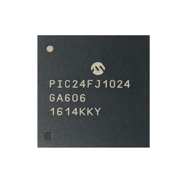
PIC24FJ1024GA606-E/MR - 16-bit 32MHz 1MB Flash MCU | Microchip
N.º da peça: PIC24FJ1024GA606-E/MR ✗ Fim de vida| Qtd. | Preço unitário | Total |
|---|---|---|
| 1 | $11.5 | $11,50 |
| 10 | $10.35 | $103,50 |
| 100 | $9.2 | $920,00 |
| 500 | $8.28 | $4.140,00 |
| 1.000 | $7.36 | $7.360,00 |
PIC24FJ1024GA606-E/MR Visão geral
A PIC microcontroller (MCU) is a compact, low-cost, programmable processor that integrates a CPU, non-volatile program storage, working RAM, and configurable peripherals onto a single silicon die. The PIC24F family from Microchip extends the 8-bit PIC16/PIC18 architecture into a 16-bit modified-Harvard core, enabling more computational throughput (measured in MIPS) and richer peripherals while preserving the deterministic interrupt model and low-power sleep modes that made the platform popular. PIC MCUs are widely used in industrial sensing, motor control, and consumer devices where ease of development, long product lifecycles, and stable supply matter more than peak raw performance.
Key features include dual-bank Flash with live update capability, on-chip ECC for higher reliability, deep sleep currents in the microamp range, and an integrated USB 2.0 full-speed OTG controller. The 16 analog channels are suitable for multi-sensor acquisition boards, while the DMA-driven peripheral set reduces CPU load in data-pump applications. The wide 3.0 V-3.6 V supply range simplifies battery-powered designs and 3.3 V point-of-load architectures.
Architecturally, the PIC24FJ1024GA606 uses a 16-bit modified-Harvard core with hardware multiply/divide, a multi-vector interrupt controller, and Microchip's PMM power management unit. The dual-partition Flash supports live update (running one bank while erasing/writing the other), enabling firmware-in-the-field upgrades without service interruption. Peripherals are routed through Microchip's PPS (Peripheral Pin Select) system, allowing flexible assignment of digital functions to most I/O pins.
Typical applications include industrial control and HMI panels, low-power IoT sensor nodes, automotive body and accessory ECUs, USB peripherals and embedded host devices, and portable medical instrumentation. For IoT designs, the combination of deep-sleep modes and live-update Flash is especially valuable - nodes can sleep for years on a single battery cell yet receive secure OTA firmware updates in the field. For industrial HMI panels, the 16 analog inputs and graphics-ready PWM timers are well-suited to touch + TFT implementations.
When designing with this MCU, pay attention to the PLL configuration sequence and the Vbat/Vddcore/Vddio decoupling layout, since high-speed ADC sampling noise can couple from digital rails. The dual-partition Flash and Live Update flow should be exercised during prototyping; failed live updates can brick the device if the bootloader is not robust.
This page synthesizes distributor pricing, drop-in same-package alternatives, and practical design notes not collected in a single place in the manufacturer datasheet.
Alternativas drop-in para PIC24FJ1024GA606-E/MR — mesmo encapsulamento, compatível pino a pino. Peças de encapsulamento diferente que exigem retrabalho na PCB são excluídas.
Variantes desta série
Modelos da mesma série compatíveis como drop-in com PIC24FJ1024GA606-E/MR (mesmo formato e footprint) — diferindo em Package, ADC, MSL Level, Core, Operating Temperature.
Ferramenta de comparação rápida — selecione peças alternativas para comparação lado a lado:
PIC24FJ1024GA606-I/MR
✓ Em estoque
$4.85 / unidade
Ver ficha técnica →PIC24FJ1024GA606-E/PT
✓ Em estoque
$5.5 / unidade
Ver ficha técnica →PIC24FJ1024GA606T-E/MR
📋 Alternativa de referência (fora do catálogo)
PIC24FJ1024GB606-I/MR
📋 Alternativa de referência (fora do catálogo)
PIC24FJ1024GA610-I/MR
📋 Alternativa de referência (fora do catálogo)
PIC24FJ1024GA606-E/MR Classificações máximas e características elétricas
| Core | PIC24 (16-bit modified Harvard) |
| CPU Architecture | 16-bit RISC, hardware multiply/divide |
| Maximum CPU Clock | 32 MHz (16 MIPS) |
| Program Memory (Flash) | 1 MB (341.5K x 24) |
| Data RAM | 32 KB |
| Flash Features | Dual Partition with Live Update and ECC |
| Supply Voltage (Vdd) | 3.0 V to 3.6 V |
| Temperatura de operação | -40C to +125C (E grade = extended) |
| UART | 6 |
| SPI | 3 |
| I2C | 3 |
| IrDA | 2 |
| PWM Channels | 6 |
| 16-bit Timers | 5 |
| Analog Comparators | 3 |
| DMA Channels | 8 |
| Analog Input Channels | 16 |
| ADC Resolution | 10/12-bit |
| USB | USB 2.0 Full-Speed OTG (on select family variants) |
| Encapsulamento | 64-QFN (MR) 9 mm x 9 mm with exposed pad |
| Tipo de montagem | Surface Mount |
| AEC-Q100 | Qualified (automotive grade) |
| Status RoHS | Compliant |
Configuração de pinos do PIC24FJ1024GA606-E/MR
| Pino 1 | RA0 — Digital I/O / analog input AN0 / PPS function |
| Pino 2 | RA1 — Digital I/O / analog input AN1 / PPS function |
| Pino 3 | RA2 — Digital I/O / analog input AN2 / PPS function |
| Pino 4 | RA3 — Digital I/O / analog input AN3 / PPS function |
| Pino 5 | RA4 — Digital I/O / analog input AN4 / PPS function |
| Pino 6 | RA5 — Digital I/O / analog input AN5 / PPS function |
| Pino 7 | RA6 — Digital I/O / analog input AN6 / PPS function |
| Pino 8 | RA7 — Digital I/O / analog input AN7 / PPS function |
| Pino 9 | VDD — Digital supply voltage (3.0 V to 3.6 V) |
| Pino 10 | VSS — Digital ground |
| Pino 11 | RB0 — Digital I/O / PGED1 / programming data |
| Pino 12 | RB1 — Digital I/O / PGEC1 / programming clock |
| Pino 13 | RB2 — Digital I/O / analog input AN8 / PPS function |
| Pino 14 | RB3 — Digital I/O / analog input AN9 / PPS function |
| Pino 15 | RB4 — Digital I/O / analog input AN10 / PPS function |
| Pino 16 | RB5 — Digital I/O / analog input AN11 / PPS function |
| Pino 17 | RB6 — Digital I/O / analog input AN12 / PPS function |
| Pino 18 | RB7 — Digital I/O / analog input AN13 / PPS function |
| Pino 19 | RB8 — Digital I/O / analog input AN14 / PPS function |
| Pino 20 | RB9 — Digital I/O / analog input AN15 / PPS function |
| Pino 21 | RC0 — Digital I/O / PPS function |
| Pino 22 | RC1 — Digital I/O / PPS function |
| Pino 23 | RC2 — Digital I/O / PPS function |
| Pino 24 | RC3 — Digital I/O / PPS function |
| Pino 25 | RC4 — Digital I/O / PPS function |
| Pino 26 | RC5 — Digital I/O / PPS function |
| Pino 27 | RC6 — Digital I/O / PPS function |
| Pino 28 | RC7 — Digital I/O / PPS function |
| Pino 29 | RC8 — Digital I/O / PPS function |
| Pino 30 | RC9 — Digital I/O / PPS function |
| Pino 31 | VSS — Digital ground |
| Pino 32 | VDD — Digital supply voltage (3.0 V to 3.6 V) |
| Pino 33 | RD0 — Digital I/O / PPS function |
| Pino 34 | RD1 — Digital I/O / PPS function |
| Pino 35 | RD2 — Digital I/O / PPS function |
| Pino 36 | RD3 — Digital I/O / PPS function |
| Pino 37 | RD4 — Digital I/O / PPS function |
| Pino 38 | RD5 — Digital I/O / PPS function |
| Pino 39 | RD6 — Digital I/O / PPS function |
| Pino 40 | RD7 — Digital I/O / PPS function |
| Pino 41 | RD8 — Digital I/O / PPS function |
| Pino 42 | RD9 — Digital I/O / PPS function |
| Pino 43 | RD10 — Digital I/O / PPS function |
| Pino 44 | RD11 — Digital I/O / PPS function |
| Pino 45 | RD12 — Digital I/O / PPS function |
| Pino 46 | RD13 — Digital I/O / PPS function |
| Pino 47 | RD14 — Digital I/O / PPS function |
| Pino 48 | RD15 — Digital I/O / PPS function |
| Pino 49 | RE0 — Digital I/O / PPS function |
| Pino 50 | RE1 — Digital I/O / PPS function |
| Pino 51 | RE2 — Digital I/O / PPS function |
| Pino 52 | RE3 — Digital I/O / PPS function |
| Pino 53 | RE4 — Digital I/O / PPS function |
| Pino 54 | RE5 — Digital I/O / PPS function |
| Pino 55 | RE6 — Digital I/O / PPS function |
| Pino 56 | RE7 — Digital I/O / PPS function |
| Pino 57 | VSS — Digital ground |
| Pino 58 | VDD — Digital supply voltage (3.0 V to 3.6 V) |
| Pino 59 | RF0 — Digital I/O / PPS function |
| Pino 60 | RF1 — Digital I/O / PPS function |
| Pino 61 | RF2 — Digital I/O / PPS function |
| Pino 62 | RF3 — Digital I/O / PPS function |
| Pino 63 | RF4 — Digital I/O / PPS function |
| Pino 64 | RF5 — Digital I/O / PPS function |
Aplicações típicas
PIC24FJ1024GA606-E/MR é adequado para 6 aplicaçãos: Industrial Control & HMI Panels, Low-Power IoT Sensor Nodes, Automotive Body & Accessory ECUs, USB Peripherals & Embedded Host, Portable Medical Instrumentation, Motor Control & Drive Boards.
Industrial Control & HMI Panels
The PIC24FJ1024GA606-E/MR fits industrial HMI panels because its 1 MB Flash holds TFT graphics frames and full Modbus stacks, while 32 KB RAM supports localized UI state. The 16 analog channels digitize potentiometer, RTD, or 4-20 mA sensor inputs directly through the 10/12-bit ADC, and the 6 PWM channels drive LED backlight dimming or small BLDC fans without an external controller. Six UARTs handle RS-232/RS-485 fieldbus bridges, while dual-partition Flash with Live Update lets the panel be reflashed in the field without service interruption - critical for factory floor downtime reduction. The 64-QFN MR package provides a compact footprint and the exposed pad enables reliable thermal dissipation inside a sealed enclosure.
Recomendado
Low-Power IoT Sensor Nodes
The PIC24FJ1024GA606-E/MR is well suited to battery-powered IoT sensor nodes because the eXtreme Low Power PIC24F core offers deep-sleep currents in the microamp range, while the 1 MB dual-partition Flash and Live Update enable OTA firmware upgrades that cannot brick deployed units. The 3 UARTs can drive a LoRa or NB-IoT module, while the 3 I2C and 3 SPI ports connect to multiple environmental sensors simultaneously. DMA channels offload sensor acquisition so the CPU spends almost all its time in sleep, extending coin-cell life into multi-year territory. The 32 KB RAM buffers a full Modbus or MQTT payload between transmit windows.
Recomendado
Automotive Body & Accessory ECUs
The PIC24FJ1024GA606-E/MR is AEC-Q100 qualified and operates over -40C to +125C, making it appropriate for body controllers, lighting modules, accessory ECUs, and HVAC panels. The 6 PWM channels drive LED matrix lighting or motor speed control; 6 UARTs interface to CAN-LIN gateways and other ECUs over the vehicle network; the 16 analog channels read potentiometers, thermistors, and battery voltage under cranking transients. Dual-partition Flash with Live Update satisfies OEM service-tool reprogramming requirements without ECU downtime, while ECC-protected Flash improves reliability in noisy under-hood electrical environments. The 64-QFN MR footprint is well established across Microchip automotive designs.
Recomendado
USB Peripherals & Embedded Host
For designs needing USB connectivity, consider the sibling PIC24FJ1024GB606 family in the same 64-QFN MR footprint, which adds a USB 2.0 Full-Speed OTG controller for both device and embedded host operation. The GA606 itself serves in peripheral designs where USB is not required but the same 1 MB Flash, 32 KB RAM, and rich peripheral set are still desired. The DMA controller handles sustained USB traffic without CPU intervention, leaving the PIC24F core free for protocol stacks or device class logic. This combination is widely deployed in USB HID, CDC, and mass-storage devices that also need multi-sensor I/O.
Recomendado
Portable Medical Instrumentation
The PIC24FJ1024GA606-E/MR supports portable medical devices such as glucose meters, pulse oximeters, and handheld patient monitors thanks to its 16 analog channels, 10/12-bit ADC resolution, and eXtreme Low Power deep-sleep modes that extend battery life between uses. The 32 KB RAM and 1 MB Flash host a real-time operating system, BLE or NFC pairing stacks, and clinical UI graphics; the 6 UARTs bridge to wireless modules for telemetry, while the 3 I2C ports handle sensor ASICs. The AEC-Q100 qualification (-40C to +125C) gives extra margin against the temperature swings of clinical environments, and dual-partition Flash supports FDA-style validated firmware updates.
Recomendado
Motor Control & Drive Boards
The PIC24FJ1024GA606-E/MR drives small BLDC, stepper, and brushed-DC motors in low-voltage applications such as appliance pumps, fans, and small robotic joints. Its 6 PWM channels with complementary outputs and programmable dead-time handle 3-phase motor commutation; 5 timers provide input capture for encoder feedback; and the DMA controller streams encoder and current-sense samples without CPU overhead. The 16 analog inputs support multi-shunt current sensing and back-EMF measurement. Dual-partition Flash lets drive firmware be tuned in the field, while ECC improves reliability against the electrical noise of switching power stages.
Recomendado
Resumo dos produtos recomendados
Dados de referência de engenharia para PIC24FJ1024GA606-E/MR — comparação, orientação de projeto e informações de conformidade.
Guia de seleção
Comparação com alternativas
| Parâmetro | Este produto | PIC24FJ1024GA606-I/MR | PIC24FJ1024GA606T-E/MR | PIC24FJ1024GB606-I/MR | PIC24FJ1024GA606-E/PT | PIC24FJ1024GA610-I/MR |
|---|---|---|---|---|---|---|
| Package | 64-QFN (MR) 9x9 mm | 64-QFN (MR) 9x9 mm - same | 64-QFN (MR) 9x9 mm - same | 64-QFN (MR) 9x9 mm - same | 64-TQFP (PT) - different | 64-QFN (MR) 9x9 mm - same |
| Brand | Microchip Technology | Microchip Technology | Microchip Technology | Microchip Technology | Microchip Technology | Microchip Technology |
| Core | PIC24F 16-bit @ 32 MHz | PIC24F 16-bit @ 32 MHz | PIC24F 16-bit @ 32 MHz | PIC24F 16-bit @ 32 MHz | PIC24F 16-bit @ 32 MHz | PIC24F 16-bit @ 32 MHz |
| Program Flash | 1 MB (dual partition, ECC) | 1 MB (dual partition, ECC) | 1 MB (dual partition, ECC) | 1 MB (dual partition, ECC) | 1 MB (dual partition, ECC) | 1 MB (dual partition, ECC) |
| RAM | 32 KB | 32 KB | 32 KB | 32 KB | 32 KB | 32 KB |
| Temperature Grade | -40C to +125C (E grade, AEC-Q100) | -40C to +85C (I grade, industrial) | -40C to +125C (E grade, AEC-Q100) | -40C to +85C (I grade, industrial) | -40C to +125C (E grade, AEC-Q100) | -40C to +85C (I grade, industrial) |
| USB 2.0 OTG | No | No | No | Yes | No | No |
| UART / SPI / I2C | 6 / 3 / 3 | 6 / 3 / 3 | 6 / 3 / 3 | 6 / 3 / 3 | 6 / 3 / 3 | 6 / 3 / 3 |
| Approx Unit Price (USD, qty 1, as of 2026-09-29) | 11.50 | 9.50 | 11.50 | 11.20 | 11.40 | 10.00 |
Principais diferenciais
- Dual-partition Flash with Live Update and ECC (vs PIC24FJ1024GA606-I/MR (industrial grade))
- AEC-Q100 automotive qualification (-40C to +125C) (vs PIC24FJ1024GA606-I/MR)
- 64-QFN (MR) 9x9 mm compact footprint (vs PIC24FJ1024GA606-E/PT (64-TQFP))
Notas de projeto
Decouple every VDD/VSS pair of the PIC24FJ1024GA606-E/MR with a 100 nF ceramic cap placed within 5 mm of each pin pair, and add a single 4.7 uF bulk capacitor near the package exposed pad. According to the PIC24FJ1024GA610/GB610 family datasheet DS30010074F, the ADC accuracy degrades noticeably when VDD ripple exceeds 50 mV during conversion. Use a star-ground topology that ties the MCU ground pin directly to the exposed pad copper pour.
The 64-QFN MR package relies on the exposed thermal pad for heat removal. Stitch a continuous ground copper pour directly under the pad with at least 16 thermal vias (0.3 mm drill, 0.6 mm pitch) to an internal ground plane. Without adequate PCB thermal dissipation, junction temperature can exceed the +125C automotive limit at sustained 32 MHz operation with all peripherals active. Estimated: at 32 MHz full-load, internal dissipation is approximately 60-80 mW; with proper PCB layout theta_JA stays below 30 C/W.
Route the ICSP pair PGEC1/PGED1 (RB1/RB0) directly to an in-circuit programming header without series resistors, and place the header at the board edge for easy probe access during manufacturing. Keep the trace length under 50 mm and avoid stubs - long ICSP traces can cause programming failures and ICE debug errors. According to the family datasheet, any PGECx/PGEDx pair can be used for ICSP but they must be used as a matched pair.
When using Live Update on the dual-partition Flash, ensure the bootloader is in a protected boot segment and implements a fail-safe rollback to the last known-good image; a failed live update without rollback can brick the device in the field. Always verify the Vbat domain is correctly bonded if RTC retention is required - leaving Vbat floating can cause unpredictable brown-out resets. The PMM must be configured per the family datasheet DS30010074F before any PLL or peripheral activation.
Separate the analog and digital ground domains on the PCB; join them at a single point under the MCU exposed pad to avoid ground-loop noise coupling into the ADC. Place the analog input traces on the opposite side of any high-speed digital signals (SPI, PWM outputs), and surround analog inputs with a guard trace tied to analog ground. Use PPS to remap noisy digital peripherals away from analog-capable pins when possible. PPS assignments should be locked early in firmware to avoid peripheral conflicts at boot.
Informações de conformidade
AEC-Q100 qualified per Hotenda listing. RoHS and REACH compliant per Microchip product page. Halogen-free status not explicitly stated in verified data.







