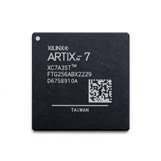
XC7A100T-1FTG256C - Artix-7 FPGA, 101K LCs, 256-FTBGA | AMD
N.º da peça: XC7A100T-1FTG256C ✓ Ativo| Qtd. | Preço unitário | Total |
|---|---|---|
| 1 | $285 | $285,00 |
| 10 | $268 | $2.680,00 |
| 100 | $252 | $25.200,00 |
| 500 | $235 | $117.500,00 |
| 1.000 | $215 | $215.000,00 |
XC7A100T-1FTG256C Visão geral
An Artix-7 FPGA is a programmable logic device that occupies the mid-range slot in AMD's 7-series portfolio (Spartan-6 below, Kintex-7 above), optimized for cost-sensitive, high-throughput, power-constrained systems. The 7-series architecture shares a unified ASMBL (Advanced Silicon Modular Block) fabric across all four family members, so Artix-7 inherits 6-input LUTs, 36 Kb block RAM, DSP48E1 slices, and SelectIO with HSTL/DDR memory interfaces from Kintex-7, while trading high-speed serial transceivers for lower die cost.
Key features include up to 6.6 Gb/s transceivers on speed-grade /package permutations (the FTG256 omits GTX), integrated PCIe Gen2 hard cores, dual 12-bit 1 Msps ADCs, and clock-management tiles comprising 6 CMTs each with one PLL and one MMCM. A 1.0 V Vccint core, separate Vccaux (1.8 V) and Vcco (1.2-3.3 V HR I/O plus 1.2-1.8 V HP I/O) rails, and an Artix-7-specific power-optimization tier let designers meet thermal envelopes as low as 2-3 W at moderate toggle rates.
Typical applications span software-defined radio (SDR) front-ends, machine-vision cameras, industrial motor control and PLCs, low-cost wireless backhaul, avionics flight controllers, and medical imaging pipelines. The FTG256 package balances thermal pad access with 170 single-ended I/Os, so most industrial and instrumentation form factors can be supported without moving to larger FGG484 or FBG676 footprints.
When designing with this device, plan decoupling around the FPGA's recommended power-rail decoupling network (one 100 uF bulk per rail plus 0.1 uF + 0.01 uF close to each VRM pin). The FTG256's 1.0 mm ball pitch supports reflow with standard 4-mil NSMD or 5-mil SMD stencils; verify thermal performance with the AMD XPE spreadsheet before committing the PCB.
This page synthesizes distributor pricing, package-level drop-in alternatives, and practical Artix-7 design notes - context not duplicated in the official ds181 datasheet.
Alternativas drop-in para XC7A100T-1FTG256C — mesmo encapsulamento, compatível pino a pino. Peças de encapsulamento diferente que exigem retrabalho na PCB são excluídas.
Variantes desta série
Modelos da mesma série compatíveis como drop-in com XC7A100T-1FTG256C (mesmo formato e footprint) — diferindo em Package.
Ferramenta de comparação rápida — selecione peças alternativas para comparação lado a lado:
XC7A100T-2FTG256C
✅ Drop-In📋 Alternativa de referência (fora do catálogo)
XC7A100T-1FTG256I
✅ Drop-In📋 Alternativa de referência (fora do catálogo)
XC7A100T-1CSG324C
✅ Drop-In✓ Em estoque
$59.9 / unidade
Ver ficha técnica →XC7A75T-1FTG256C
✅ Drop-In📋 Alternativa de referência (fora do catálogo)
LFE5U-100F8BG756I
✅ Drop-In📋 Alternativa de referência (fora do catálogo)
XC7A100T-1FTG256C Classificações máximas e características elétricas
| Family | Artix-7 |
| Logic Cells | 101,440 |
| Block RAM (bits) | 4,976,640 |
| Block RAM (Kb) | 4,860 |
| DSP Slices (DSP48E1) | 240 |
| Speed Grade | -1 |
| Temperature Grade | Commercial (C): 0 C to +85 C |
| Encapsulamento | 256-ball FTBGA (FTG256) |
| Package Size | 17 mm x 17 mm, 1.0 mm pitch |
| User I/Os | 170 |
| CMTs (PLL + MMCM) | 6 |
| Process Node | 28 nm HPL HKMG |
| Core Voltage (Vccint) | 1.0 V nominal |
| Auxiliary Voltage (Vccaux) | 1.8 V nominal |
| Configuration Mode | Master Serial / Slave Serial / SPI / BPI / JTAG |
| Status RoHS | Compliant |
| Tipo de montagem | Surface Mount (BGA) |
Guia de Configuração de Pinos do XC7A100T-1FTG256C 17 mm x 17 mm, 1.0 mm pitch
Configuração de pinos para XC7A100T-1FTG256C (pacote 17 mm x 17 mm, 1.0 mm pitch). Este CI digital inclui GPIO, interfaces de comunicação (UART, SPI, I2C) e pinos de alimentação. Consulte o datasheet do fabricante para funções alternativas dos pinos e opções de configuração. Essencial para projeto de sistemas embarcados e layout de PCB.

Nenhum dado detalhado de pinagem disponível para XC7A100T-1FTG256C.
Consulte a ficha técnica para a configuração completa dos pinos.
Aplicações típicas
XC7A100T-1FTG256C é adequado para 6 aplicaçãos: Software Defined Radio (SDR), Machine Vision Camera Processing, Industrial Motor Control, Software Defined Wireless Backhaul, Medical Imaging Front End, Avionics Flight Control & Drones.
Software Defined Radio (SDR)
The XC7A100T-1FTG256C's 240 DSP48E1 slices and 4,976,640 bits of block RAM make it a strong fit for SDR baseband and IF processing in commercial-grade platforms. The FTG256's 170 user I/Os provide enough LVDS pairs to interface a 16-bit dual-channel ADC at up to 250 Msps for narrowband IF sampling, while the -1 speed grade meets timing for lattice-based channelizers. The 28 nm HPL process keeps typical SDR board power below 4-5 W, beating Spartan-6 perf/W by ~40%. Use MMCMs for sampling-clock synthesis and allocate spare block RAM for polyphase filterbanks. Avoid the FTG256 footprint if you need >4 Gbps serial links - that requires GTX transceivers found only on higher packages.
Recomendado
Machine Vision Camera Processing
The XC7A100T-1FTG256C delivers ample logic and 240 DSP48E1 slices for real-time image processing in industrial cameras: Bayer demosaicing, color correction, and Sobel/FFT kernels run comfortably within ~60 percent of the 100T's resources at 1080p60. The FTG256's 17x17 mm body fits inside PoE-plus camera heads where board area is constrained, while 170 user I/Os accommodate MIPI-CSI, LVDS, and HD-SDI sensor inputs. Industrial-grade variants (XC7A100T-1FTG256I) extend operation into -40 C to +100 C workshops. Power optimization techniques - clock-gating, GT-disabled bitstreams, and DPRIO-mode block RAM banking - keep camera head dissipation under 3.5 W for fanless designs.
Recomendado
Industrial Motor Control
Industrial motor drives benefit from the XC7A100T-1FTG256C's high DSP48E1 count for field-oriented control (FOC) loops at switching frequencies up to 50 kHz. The -1 commercial speed grade is sufficient for sinusoidal encoder interpolation when the FPGA over-samples quadrature signals; the 240 DSP slices handle 4-6 sensorless observers per device. The FTG256 exposes enough HP I/Os to drive 12-channel three-phase MOSFET gate drivers directly, while Vcco can be split between 3.3 V for logic and 1.8 V for high-speed ADCs. For harsh industrial environments, the XC7A100T-1FTG256I industrial variant supports -40 C operation. Validate temperature with the AMD XPE spreadsheet at full DSP utilization.
Recomendado
Software Defined Wireless Backhaul
Low-cost wireless backhaul radios (sub-6 GHz LTE/5G small cells, TVWS, point-to-point microwave) find a sweet spot in the XC7A100T-1FTG256C's resource mix. The 101K logic cells support CPRI/SERDES interfaces at half-rate plus baseband PHY functions, while block RAM allocates happily to OFDM CP/FFT scratch buffers. The FTG256's 17 mm footprint fits in the industry-standard micro-onu form factor used in small-cell radios, and 170 I/Os support multi-radio JESD204B ADC hook-ups at 3 Gbps. The -1 commercial grade satisfies indoor and weatherproof-enclosure deployments; choose XC7A100T-1FTG256I for outdoor i-3 cabinet gear.
Recomendado
Medical Imaging Front End
The XC7A100T-1FTG256C's 240 DSP slices and 4.86 Mb block RAM suit portable medical imaging - ultrasound beamforming, optical coherence tomography (OCT), and pulse-oximetry DSP pipelines. The FTG256's compact 17 mm package and 170 I/Os allow a portable handheld imaging head to integrate multiple ADCs without PCB area scaling. Decoupling rails with low-noise LDOs (TPS7A4700 family) preserves ADC dynamic range - SNR improvement of 3-5 dB over switching-only supplies is achievable. FDA/IEC 60601-1 isolation requirements dictate that any medical design uses the industrial-grade XC7A100T-1FTG256I; the commercial grade is limited to non-life-support clinical equipment.
Recomendado
Avionics Flight Control & Drones
Small UAV flight controllers and Experimental aircraft attitude reference systems fit the XC7A100T-1FTG256C's resource envelope: redundant sensor arbitration (IMU + GPS + barometer + magnetometer) and Kalman filtering run comfortably in <20 percent of logic, leaving headroom for custom control laws. The FTG256's 17 mm footprint suits PC/104-class boards used in experimental avionics, while 170 I/Os support up to 4x CAN, 2x Ethernet MAC interfaces, and 8 PWM-driven motor esc lines. Pair with industrial XC7A100T-1FTG256I for -40 C to +100 C operational envelopes demanded by low-altitude flight electronics. Note that DO-254 certifiable projects require additional documentation beyond standard FPGA design packages.
Recomendado
Resumo dos produtos recomendados
Dados de referência de engenharia para XC7A100T-1FTG256C — comparação, orientação de projeto e informações de conformidade.
Guia de seleção
Comparação com alternativas
| Parâmetro | Este produto | XC7A100T-2FTG256C | XC7A100T-1FTG256I | XC7A100T-1CSG324C | XC7A75T-1FTG256C | LFE5U-100F8BG756I |
|---|---|---|---|---|---|---|
| Brand | AMD | AMD | AMD | AMD | AMD | Lattice Semiconductor |
| Package | 256-ball FTBGA (FTG256) 17x17 mm | 256-ball FTBGA (FTG256) 17x17 mm - same | 256-ball FTBGA (FTG256) 17x17 mm - same | 324-ball CSBGA (CSG324) 12x12 mm | 256-ball FTBGA (FTG256) 17x17 mm - same | 256-ball BGA - cabGA variant |
| Logic Cells | 101,440 | 101,440 | 101,440 | 101,440 | 75,520 | 100K LUTs |
| DSP Slices | 240 | 240 | 240 | 240 | 180 | 196 SYS DSP blocks |
| Block RAM (bits) | 4,976,640 | 4,976,640 | 4,976,640 | 4,976,640 | 3,780,000 | 3,750,000 |
| User I/Os | 170 | 170 | 170 | 210 | 170 | 248 |
| Speed Grade | -1 | -2 | -1 | -1 | -1 | LFE5U 8G turbo |
| Temperature Grade | Commercial 0 C to +85 C | Commercial 0 C to +85 C | Industrial -40 C to +100 C | Commercial 0 C to +85 C | Commercial 0 C to +85 C | Industrial -40 C to +100 C |
Principais diferenciais
- Highest logic/DSP density in 256-ball FTBGA class for cost-sensitive designs (vs XC7A75T-1FTG256C)
- Compact 17x17 mm body for high-density board designs (vs XC7A100T-1CSG324C)
- AMD Xilinx toolchain maturity including Vivado WebPACK free licensing (vs LFE5U-100F8BG756I)
Notas de projeto
Estimated: The Artix-7 FTG256 junction-to-ambient thermal resistance (theta_JA) for a standard 4-layer JEDEC test board is ~13 C/W with the center thermal balls connected, so a fully loaded 100T at 1 W dissipation rises only ~13 C above ambient. For sealed enclosures with limited convection, the AMD XPE spreadsheet predicts a more realistic 2-3 W steady-state power budget; add 1 mm copper clearances above the ball grid to expose the thermal balls for a heat spreader.
Decoupling per the AMD Xilinx UltraScale/7-series reference design: one 100 uF bulk capacitor + one 4.7 uF + one 0.1 uF + one 0.01 uF capacitor stack per Vccint pin pair, placed within 1 cm of the BGA balls. Vccaux requires a 4.7 uF + 0.1 uF stack per ball; Vcco banks each need 0.1 uF close to every four pins. Use 4-mil NSMD land pads on a 1.0 mm BGA pitch and standard 4-mil stencils for assembly.
Do not assume GTX transceivers are present on FTG256 - the 100T FTG256 omits GTX; only specific Kintex-7 packages expose multi-gigabit transceivers. If your design needs >500 Mbps serial links, you must select a Kintex-7 or move to a Spartan-7 with limited 1.25 Gbps SERDES, or implement LVDS-based communications. For JTAG, route TCK with a series 100-ohm termination at the FPGA end to prevent signal ringing on long scan chains.
Informações de conformidade
RoHS and REACH compliance per AMD product page. Not AEC-Q100 qualified - the device is for industrial / commercial systems; equivalent automotive XA7A100T variants exist on the XA prefix.