Транзисторы
Товары (115)

STBV45 - 400V NPN High-Voltage Fast-Switching BJT | STMicroelectronics
The STMicroelectronics STBV45 is a high-voltage, fast-switching NPN bipolar junction transistor rated at 400 V VCEO/VCBO, 750 mA collector current, and 950 mW power dissipation, housed in a TO-92-3 through-hole package. It uses high-voltage multi-epitaxial planar technology to deliver high switching speeds while maintaining high voltage capability, and employs a cellular emitter structure with planar edge termination to enhance switching speed and widen the reverse-biased safe operating area (RBSOA). A BJT (bipolar junction transistor) is a three-terminal semiconductor device that uses a small base current to control a much larger collector current, enabling amplification and high-speed switching. The NPN variant conducts when the base is pulled above the emitter, making it the natural choice for low-side switching in positive-rail circuits. Within the broader taxonomy, BJTs sit alongside MOSFETs and IGBTs in the discrete-semiconductor family, with BJTs typically preferred where cost, saturation behavior, or ruggedness in fault conditions outweigh the need for ultra-low gate drive power. Key features of the STBV45 include a minimum DC current gain (hFE) of 8 at IC = 250 mA, low spread of dynamic parameters for predictable switching, and minimum lot-to-lot variation for reliable high-volume manufacturing. The TO-92-3 package offers three through-hole leads (collector, base, emitter) suited for hand-soldered prototyping and low-cost PCB designs. The 950 mW power dissipation rating requires careful thermal management when operating near maximum collector current. From a switching perspective, the STBV45 is designed for compact fluorescent lamp (CFL) ballasts and SMPS battery-charger primary-side switching where high-voltage breakdown and fast turn-off are required simultaneously. The cellular emitter layout keeps storage and fall times short, reducing switching losses at elevated frequencies. Designers typically operate this transistor at VCEO derated to roughly 60% of his design limit, and pair it with a base-drive network sized to saturate the device at the desired collector current. Typical applications include compact fluorescent lamps (CFLs), switching-mode power supplies (SMPS) for battery chargers, and high-voltage electronic lighting ballasts. The wide low-voltage footprint and robust RBSOA make it a common choice for cost-sensitive offline switching converters. When designing with the STBV45, ensure the base-drive resistor is sized to provide sufficient base current at minimum hFE, and confirm that the switching frequency stays within the device's safe operating area to avoid second-breakdown failures.
STBV45-AP - 400V NPN High-Voltage Fast-Switch Transistor | STMicroelectronics
The STMicroelectronics STBV45-AP is a high-voltage fast-switching NPN bipolar power transistor housed in a TO-92AP (Ammopack) through-hole package. It is rated for a collector-emitter voltage (VCEO) of 400 V, a collector current (IC) of 0.75 A, and is engineered for very high switching speed with low spread of dynamic parameters across the lot, making it a reliable choice for repetitive high-voltage switching applications. The device uses high-voltage multi-epitaxial planar technology with a cellular emitter structure and planar edge termination, achieving wide Reverse Bias Safe Operating Area (RBSOA) and tight switching parameter distribution. A bipolar junction transistor (BJT) is a three-terminal semiconductor device formed by two PN junctions that operates by injecting minority carriers across a base region to control a much larger collector current. NPN BJTs like the STBV45-AP are particularly suited to high-voltage, fast-switching roles because the multi-epitaxial planar process supports high breakdown voltages while maintaining short carrier transit times. Within the broader component taxonomy, the STBV45-AP is a discrete semiconductor -> transistor -> bipolar transistor (BJT) -> NPN power transistor, serving power conversion and switch-mode sub-systems rather than small-signal amplification. Key features of the STBV45-AP include a 400 V VCEO rating, 0.75 A continuous collector current, very high switching speed enabled by the cellular emitter, low lot-to-lot dynamic parameter spread, minimum dynamic parameter spread for predictable paralleling or sequencing, a wide Reverse Bias Safe Operating Area for inductive load commutation, and the planar edge termination that improves voltage stability at the silicon surface. The TO-92AP (Ammopack) radial lead package supports automated axial-style insertion or hand soldering in compact lighting and charger modules. The device is built using high-voltage multi-epitaxial planar technology for high switching speeds and high voltage capability, and uses a cellular emitter structure with planar edge termination to enhance switching speeds while maintaining the wide RBSOA. This combination makes the part attractive for switch-mode power topologies where predictable turn-off behaviour under inductive loads is critical. Typical applications include compact fluorescent lamps (CFLs), SMPS (switch-mode power supply) for battery chargers, electronic ballasts, high-voltage DC-DC converters, and inductive heating driver stages. It is also commonly used in flyback and forward converters, line-powered switching regulators, and any circuit that requires switching 200-400 V rails with a low-cost discrete BJT. When designing with the STBV45-AP, attention must be paid to safe operating area under reverse-bias conditions, to base-drive turn-off speed, and to thermal management through the TO-92 leads since the package does not have a heatsink tab. A sufficiently large snubber or clamp network is recommended when switching inductive loads near the VCEO limit. This page synthesizes distributor pricing, drop-in alternatives from the same family, and practical design notes for high-voltage BJT switching not found in the manufacturer datasheet alone.
STL73-AP - 400V 1.5A NPN Power Transistor | STMicroelectronics
The STMicroelectronics STL73-AP is a medium-voltage, fast-switching NPN bipolar junction transistor (BJT) housed in a 3-pin TO-92 plastic package with formed leads for through-hole mounting. It offers a maximum collector-emitter voltage (VCEO) of 400V, a continuous collector current (IC) of 1.5A, and a maximum power dissipation of 1100 mW (1.1 W), making it well suited to general-purpose medium-voltage switching and linear applications. A BJT (bipolar junction transistor) is a three-terminal semiconductor device that amplifies current or switches signals using both electron and hole charge carriers. Within the broader semiconductor hierarchy, the BJT sits as a sibling technology to MOSFETs and IGBTs in the discrete-transistor family, while within STMicroelectronics' portfolio the STL73 belongs to the medium-voltage fast-switching NPN power transistor group, engineered using the company's Multi-Epitaxial Planar process to combine high switching speed with 400V breakdown capability. Key features of the STL73-AP include a 400V VCEO rating that comfortably supports 110V/220V offline-derived rails after rectification, a 1.5A continuous collector current suitable for relay coils, solenoid drivers, and small motor windings, and a 1100 mW power dissipation envelope that allows sustained operation without an external heatsink in typical low-duty-cycle use. The device operates across an extended -65°C to +150°C junction temperature range, ensuring reliability in automotive underhood, industrial, and consumer environments. The Multi-Epitaxial Planar architecture provides a balanced trade-off between breakdown voltage, current handling, and switching speed, which is why the part is specified for fast-switching applications rather than pure RF or precision linear use. Compared with a generic 400V small-signal transistor, the STL73-AP offers substantially higher collector current and dissipation, and its TO-92 form factor preserves drop-in compatibility with legacy through-hole designs that would otherwise require a footprint change. Typical applications include line-powered switch-mode power supply (SMPS) auxiliary circuits, electronic ballast control stages, LED driver buck/boost stages, solenoid and relay drivers, and general-purpose medium-voltage amplifiers. The combination of 400V breakdown and 1.5A current also suits the part for use as a driver transistor for higher-power devices such as MOSFETs or TRIACs in offline control circuits. When designing with the STL73-AP, derate power dissipation to 600-700 mW in most TO-92 layouts without a copper heatsink pad, since the TO-92 package has a thermal resistance of approximately 200 C/W to ambient. Always observe safe operating area limits when switching inductive loads, and add a flyback or snubber diode across any inductive load to protect the collector-base junction from reverse breakdown transients. This page synthesizes distributor pricing, drop-in alternatives, and practical design notes not found in the manufacturer datasheet alone, giving engineers a single reference for sourcing, substitution, and layout guidance.
STX83003-AP - 400V NPN High-Voltage Fast Switch BJT | STMicro
The STMicroelectronics STX83003-AP is a 400 V, 1 A NPN bipolar junction transistor built on high-voltage Multi Epitaxial Planar technology and housed in a TO-92-3 through-hole package with Ammo Pack (AP) tape packaging. Designed for high switching speeds and medium voltage capability, the device uses a Cellular Emitter structure with planar edge termination to enhance switching speeds while maintaining a wide Reverse Bias Safe Operating Area (RBSOA). What is a high-voltage fast-switching NPN BJT? It is a bipolar junction transistor whose collector-emitter breakdown voltage (VCEO) is rated at several hundred volts while still providing sub-microsecond fall times, enabling efficient drive of inductive loads such as fluorescent lamp ballasts, deflection circuits, and switching-mode power supply snubbers. Within the transistor hierarchy, this places STX83003-AP as NPN BJT -> bipolar transistor -> discrete semiconductor -> semiconductor device. Key specifications include a collector-emitter breakdown voltage of 400 V, continuous collector current of 1 A, total power dissipation of 1.5 W in free air, DC current gain (hFE) minimum of 16 at 350 mA / 5 V, and a low VCE saturation characteristic that minimizes conduction loss in switching applications. The TO-92-3 package is the industry-standard through-hole outline, allowing PCB replacement without footprint rework for designers migrating from legacy ZTX or MPSA-style high-voltage transistors. Architecture-wise, the Multi Epitaxial Planar process delivers narrow dynamic-parameter spread and minimum lot-to-lot spread for reliable operation across production batches. The Cellular Emitter geometry and planar edge termination suppress localized hot-spotting at high dV/dt, supporting a wide RBSOA that is critical when the transistor turns off inductive loads where the collector voltage spikes above the DC rail. Typical applications include electronic ballasts for fluorescent lighting, switching regulators, high-voltage DC-DC converters, deflection circuits for CRT displays, and general-purpose medium-voltage N power switching where a small-signal BJT such as the 2N5551 lacks voltage headroom. Compared with the surface-mount STN83003 in SOT-223, the STX83003-AP offers a TO-92 through-hole form factor favored by hobbyist, replacement, and through-hole industrial designs. Designers should observe a maximum junction temperature of 150°C and derate dissipation according to the TO-92 thermal resistance (approximately 200°C/W free air). A small clip-on heatsink or PCB copper thermal relief noticeably improves RBSOA margin in continuous high-voltage switching service. A base-drive resistor of 1 kΩ to 10 kΩ is recommended to control turn-off dV/dt and limit stored base charge. This page combines distributor pricing, parametric comparison with drop-in equivalents, and design guidance not consolidated in the manufacturer datasheet.

TIP31C - NPN 100V 3A Power Transistor TO-220 | STMicroelectronics
The STMicroelectronics TIP31C is an NPN bipolar junction power transistor rated for 100 V collector-emitter voltage and 3 A continuous collector current, housed in a through-hole TO-220 plastic package. Manufactured with base island technology, this device delivers better switching and linear performance than the industry-standard TIP31C it supersedes. A BJT power transistor is a three-terminal semiconductor that uses a small base current to control a much larger collector current, making it the workhorse of medium-power amplification and switching. Within the power management hierarchy, the TIP31C sits in the discrete transistor family that spans from small-signal BJTs up to high-current Darlington devices, and it is complemented by the PNP TIP32C for push-pull designs. Key features include a 100 V VCEO rating that provides ample margin on 48 V-class rails, a 3 A continuous collector current with peak capability up to 5 A per the ST datasheet family rating, a DC current gain (hFE) of at least 10 at 3 A, and a transition frequency of 3 MHz. The base island technology construction lowers saturation voltage and improves switching behavior compared with conventional epitaxial designs. Technically, the TIP31C uses an epitaxial-base NPN silicon structure optimized for both linear and switching service. Power dissipation is rated at 40 W at a case temperature of 25 C when properly heatsinked (approximately 2 W free-air per distributor listings), so thermal design determines real usable output. Typical applications include audio amplifier output stages, general-purpose linear regulators, relay and solenoid drivers, motor drivers, and medium-speed power switching circuits. When designing with the TIP31C, verify the safe operating area at your actual case temperature and drive the base with sufficient current to keep hFE-related saturation losses low; a forced beta of 10 is the usual rule of thumb. This page synthesizes distributor pricing, drop-in alternatives, pinout details, and practical design notes not found in the manufacturer datasheet alone.
TIP41C - 100V 6A NPN Power BJT TO-220 | STMicroelectronics
The STMicroelectronics TIP41C is an NPN bipolar junction power transistor rated 100 V collector-emitter voltage, 6 A continuous collector current, and 65 W power dissipation, housed in a 3-pin TO-220 (TO-220AB) through-hole package with exposed collector tab. Its complementary PNP counterpart is the TIP42C. A power BJT (bipolar junction transistor) is a current-controlled semiconductor switch and amplifier that sits at the top of the transistor hierarchy: transistor -> bipolar junction transistor -> power BJT. Unlike MOSFETs, BJTs are driven by base current and offer robustness against static discharge, making them a staple in medium-power linear and switching stages. Key features include base island technology, which STMicroelectronics uses to reduce thermal resistance and improve switching behavior; a 65 W dissipation rating at a properly heatsinked case; and broad availability from multiple second sources, which reduces supply risk in long-lifecycle industrial designs. The TO-220 package mounts to standard heatsinks with a single screw and insulated kit. Technically, the TIP41C is fabricated on a base island process that minimizes internal parasitic resistance, allowing high collector current with moderate DC current gain. The 'C' suffix denotes the 100 V voltage grade in the TIP41 series (A = 40 V, B = 60 V, C = 100 V), so lower-grade variants must never be substituted in 100 V rails. Typical applications include linear audio amplifier output stages, general-purpose power linear regulation, relay and solenoid drivers, and low-frequency switching power supplies where the rugged, well-understood BJT behavior is preferred over a MOSFET. Design consideration: because BJT gain (hFE) falls sharply at high collector current, budget ample base drive current - typically 600 mA or more for a 6 A load - and verify safe operating area margins when switching inductive loads. A snubber or flyback diode is recommended for inductive switching. This page adds value beyond the manufacturer datasheet by synthesizing drop-in alternatives, pinout details, design notes, and pricing tiers in one place for engineering and sourcing teams.
TIP41C-BP - NPN 100V 6A Power BJT TO-220AB | MCC
The MCC (Micro Commercial Components) TIP41C-BP is an NPN bipolar junction power transistor rated for 100 V collector-emitter breakdown voltage, 6 A maximum continuous collector current, and 65 W power dissipation at a case temperature of 25 C, housed in a through-hole TO-220AB (TO-220) package with a 3 MHz transition frequency. A bipolar junction transistor (BJT) is a three-terminal current-controlled semiconductor device that amplifies or switches electronic signals. Within the component hierarchy, the TIP41C-BP belongs to the general-purpose power BJT family, sitting under discrete transistors, under discrete semiconductors, and ultimately under power electronics. Power BJTs remain popular where simple, robust, low-cost drive circuits are needed, complementing MOSFETs and IGBTs in the broader power device landscape. Key features include a 100 V VCEO rating for headroom on industrial supply rails, a 6 A collector current capability, a minimum DC current gain (hFE) of 15 at 3 A and 4 V, and a 3 MHz transition frequency that supports medium-speed switching. The P suffix designates RoHS-compliant lead-free construction per the manufacturer datasheet ordering information. The TIP42 series PNP device is its complementary pair. The device uses a planar NPN structure optimized for linear and switching service. Its TO-220AB package with exposed collector tab provides a low-resistance thermal path to a heatsink; note that the 65 W rating applies at maintained case temperature of 25 C, while free-air dissipation without heatsinking is far lower (DigiKey lists 2 W as the free-air figure), so thermal design drives real-world capability. Typical applications include linear power supplies and series pass elements, motor drivers and relay/actuator drivers, audio power amplifier output stages, and general medium-power switching in industrial equipment. Design consideration: always verify SOA and heatsink requirements at your actual Vce and Ic operating point, because second breakdown limits BJT safe operating area at high voltage and high current simultaneously. This page synthesizes verified distributor data, drop-in alternatives, pinout information, and practical thermal design notes not found in a single manufacturer datasheet.
TIP41C-SL-PBFREE - NPN 100V 6A 65W BJT | Central Semiconductor
The Central Semiconductor TIP41C-SL-PBFREE is an NPN epitaxial-base silicon power bipolar junction transistor (BJT) rated for 100 V collector-base voltage (Vcbo), 100 V collector-emitter voltage (Vceo), 5.0 V emitter-base voltage (Vebo), 6 A continuous collector current, and 65 W power dissipation at 25 C case temperature, housed in a through-hole TO-220-3 package. A power BJT is a current-controlled semiconductor device that amplifies or switches electrical power in the final stage of a system hierarchy that runs from discrete transistors up to power amplifier and motor-drive circuits. Unlike MOSFETs, BJTs require base drive current proportional to collector current divided by current gain (hFE), which makes them simple to drive from op-amps or logic through a resistor, and gives them well-behaved, linear transfer characteristics favored in analog power stages. Key features of the TIP41C-SL-PBFREE include its 100 V breakdown ratings (the C suffix denotes the highest-voltage gain group of the TIP41 family), a transition frequency of 3 MHz supporting high-speed switching, and the 65 W package dissipation enabled by the metal-tab TO-220 construction. The PBFREE suffix indicates a lead-free, RoHS-oriented plating system without lead content. Technically, the device uses an epitaxial-base silicon process optimized by Central Semiconductor for power amplifier and high-speed switching applications, per the manufacturer TIP41-series datasheet. The NPN polarity provides positive-side sourcing capability and pairs naturally with the complementary PNP TIP42C in push-pull or Class AB output stages. Typical applications include linear power amplifier output stages, medium-power switching regulators, DC motor drivers, solenoid and relay drivers, and general-purpose amplification in industrial and consumer equipment. A key design consideration is thermal management: the 65 W rating applies only with the case held at 25 C, so practical designs must calculate junction temperature using the package thermal resistance and provide an adequately sized heatsink. Estimated: at 6 A and 100 V ceiling designs, real dissipation should be budgeted well below 65 W in still air. This page adds value beyond the datasheet by synthesizing distributor pricing, verified drop-in alternatives across brands, and practical thermal and layout design notes in one place.
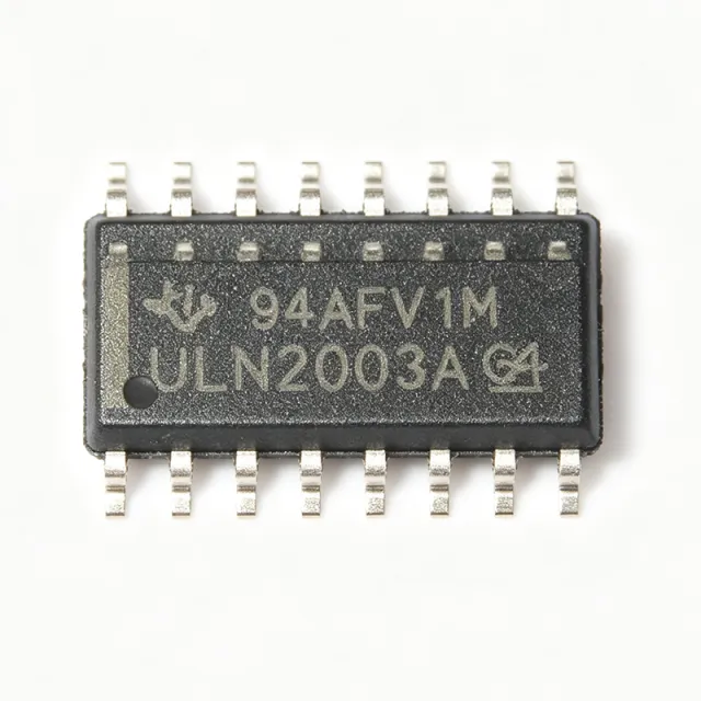
ULN2003AD - 7-Channel Darlington Driver | Texas Instruments
The Texas Instruments ULN2003AD is a 7-channel high-voltage, high-current Darlington transistor array designed for driving inductive loads such as relays, solenoids, stepper motors, and lamps. It features seven open-collector Darlington pairs with common-cathode clamp diodes for inductive transient suppression, and is available in a 16-pin SOIC (D) package. Each channel can sink up to 500 mA continuously and 600 mA peak, with a collector-emitter voltage rating of 50 V. The device operates over a temperature range of -40°C to +105°C and is RoHS compliant. A Darlington transistor array is a semiconductor device that integrates multiple Darlington pairs, each consisting of two bipolar transistors in a configuration that provides high current gain. This category falls under the hierarchy: Darlington array -> transistor array -> discrete semiconductor -> semiconductor. The ULN2003A is a specific variant of the ULN2003 family, which is widely used in industrial and consumer applications for interfacing low-level logic signals to high-current loads. Key features include seven Darlington pairs with a total current capability of 500 mA per channel, a collector-emitter voltage rating of 50 V, and integrated clamp diodes for inductive load protection. The input is compatible with TTL and 5V CMOS logic, and the device includes a common emitter for all channels. The SOIC-16 package provides a compact footprint for space-constrained designs. The ULN2003AD uses a bipolar process technology with a high-current NPN Darlington configuration. Each channel has a base resistor (2.7 kΩ) and an emitter resistor (3.6 kΩ) to ensure proper biasing and thermal stability. The integrated clamp diodes are connected to a common cathode pin (pin 9) for easy connection to the supply rail. The device exhibits a low saturation voltage (typically 1.6 V at 350 mA) to minimize power dissipation. Typical applications include relay drivers, stepper motor drivers, solenoid drivers, and lamp drivers in industrial control, automotive, and consumer electronics. The high current gain allows direct interfacing with microcontrollers without additional driver stages, simplifying circuit design. When designing with this device, ensure that the total power dissipation does not exceed the package thermal limits. For high-current applications, consider using multiple channels in parallel or adding external heatsinking. The clamp diodes must be connected to the positive supply rail to protect against inductive kickback. This page synthesizes distributor pricing, drop-in alternatives, and practical design notes not found in the TI datasheet, providing a comprehensive resource for engineers selecting the ULN2003AD.

ULN2003ADR - 50V 500mA 7-ch Darlington Array SOIC-16 | TI
The Texas Instruments ULN2003ADR is a high-voltage, high-current Darlington transistor array containing seven NPN Darlington pairs in a 16-pin SOIC (D) surface-mount package. Each channel is rated for 500 mA collector current and 50 V collector-emitter voltage, with integrated common-cathode clamp diodes for inductive load driving. The device includes 2.7 kOhm series base resistors on every input, allowing direct interface with TTL or CMOS logic at 3.3 V or 5 V without external components. A Darlington transistor array is a monolithic IC that integrates multiple high-gain Darlington-pair switches, each formed by two cascaded bipolar transistors whose collectors tie together and whose emitters drive the load. Within the broader taxonomy, the ULN2003ADR sits under: transistor array -> bipolar transistor array -> Darlington array -> driver IC -> semiconductor. Each pair typically delivers beta > 1000, so a few milliamps of input current can switch hundreds of milliamps at the output. This integration simplifies board design by replacing seven discrete NPN transistors plus seven base resistors with a single 16-pin IC. Key features include 500 mA continuous collector current per channel, 50 V minimum output breakdown, integrated flyback diodes, and logic-level inputs compatible with 3.3 V and 5 V microcontrollers. The open-collector outputs allow flexible pull-up voltage selection independent of the logic supply. The SOIC-16 (D) package offers a small footprint suitable for reflow soldering, with all seven channels and the common-cathode clamp brought out for easy PCB routing. The architecture is bipolar; the seven Darlington pairs share a common emitter (substrate) tied to the GND pins. Total power dissipation for the package is approximately 0.95 W at 25 C, derating linearly with temperature. Channel-to-channel matching is tight because all pairs share the same silicon die, which is critical for stepper motors and multi-coil relay banks requiring matched drive strength. Typical applications include unipolar stepper motor drivers, relay and solenoid drivers, lamp and LED matrix drivers, and logic-level buffers for higher-current loads. In each case the ULN2003ADR replaces discrete driver circuits with a single IC, reducing PCB area and BOM count. When designing with this device, ensure that the total package dissipation stays below the derated limit by calculating the worst-case voltage drop across each conducting Darlington and summing across active channels. The clamp diodes handle inductive kickback, but the user must still size the supply decoupling appropriately for the load.

ULN2003AN - 50V 500mA 7-Ch Darlington Array | TI | DIP-16
The Texas Instruments ULN2003AN is a high-voltage, high-current Darlington transistor array consisting of seven open-collector NPN Darlington pairs rated at 50V and 500 mA per channel, housed in a 16-pin PDIP (N) through-hole package. Each pair integrates two bipolar transistors in a Darlington configuration, yielding typical current gain of approximately 1000 (beta min 1000 per the manufacturer datasheet) at low input currents, allowing direct drive from CMOS, TTL, and 5V microcontrollers. Integral common-cathode clamp diodes tied to a dedicated COM pin permit direct switching of inductive loads such as relay coils, unipolar stepper motors, and solenoids without external freewheeling circuitry. A Darlington transistor array is a class of bipolar (BJT) integrated circuit that bundles multiple high-gain Darlington pairs on a single die, acting as a low-side driver. Within the broader taxonomy, it belongs to the discrete transistor category, sits below generic BJT arrays, and is widely classified as an interface/driver IC for relay, lamp, and motor loads. The ULN2003 family is the de-facto industry standard for 7-channel low-side switching from logic-level inputs, making it one of the longest-lived and most cloned ICs in the market. Key features include seven identical Darlington output stages, 50V minimum collector-emitter sustaining voltage, 500 mA continuous collector current per channel (peak to 600 mA), built-in output clamp diodes for inductive load protection, inputs compatible with TTL/CMOS/PMOS/DTL logic, and an operating junction temperature range up to 150 C. The input pins present a series base resistor suitable for 3.3V and 5V logic; no external resistor network is required. Architecturally, each channel pairs a driver transistor (Q1) and an output transistor (Q2) to multiply beta, with integrated 2.7 kohm base resistors on every input. This monolithic bipolar process yields predictable saturation behavior (Vce(sat) ~0.9-1.0V at low currents, ~1.1V at 350 mA) but introduces a measurable Vce drop that dissipates substantial power in high-current applications. Typical applications include 5V relay driver cards, unipolar stepper motor driver boards (commonly paired with 28BYJ-48 motors), LED matrix row/column drivers, solenoid valves, DC brushed motor direction switches, and lamp/display drivers. Hobby and educational platforms (Arduino shields, Raspberry Pi HATs) frequently adopt the ULN2003AN because of its robust 500 mA rating and zero-firmware footprint. Designers should budget headroom for the ~1V collector-emitter saturation drop and derate output current as duty cycle rises. The thermal resistance of PDIP-16 (theta_JA ~70 C/W typical) limits total package dissipation to roughly 1.5W without airflow, so high-current loads should be distributed across multiple channels rather than concentrated on a single pair. This page synthesizes distributor pricing for the original TI part plus cloned second-source options, a drop-in alternative table for sourcing resilience, and practical PCB/application guidance beyond what the manufacturer datasheet covers in isolation.
ULN2003ANE4 - 7-Ch NPN Darlington 500mA 16-PDIP | TI
The Texas Instruments ULN2003ANE4 is a high-voltage, high-current Darlington transistor array containing seven NPN Darlington pairs in a 16-pin PDIP through-hole package. Each channel is rated for 50V collector-emitter breakdown and 500mA continuous collector current, with built-in common-cathode clamp diodes for inductive load switching. The input pins are designed for direct CMOS, TTL, and 3.3V MCU logic interfacing through integrated base resistors. A Darlington transistor array is a monolithic IC that integrates multiple Darlington-pair drivers in a single package, allowing microcontrollers and low-power logic to switch high-current loads such as relays, solenoids, lamps, and stepper motor windings. Each Darlington pair multiplies the input current by the product of the two transistor betas, producing very high current gain (typically 10,000+) and enabling a logic-level signal to drive loads drawing hundreds of milliamps. The ULN2003 family sits at the low-side (open-collector) side of an H-bridge or relay driver topology, and is widely recognized as the de-facto standard driver for Arduino relay boards, 28BYJ-48 stepper motors, and unipolar stepper motor control. Key features include 7 matched channels with 500mA per-channel continuous rating, integrated 2.7kOhm base resistors for direct 5V/3.3V logic interface, built-in freewheeling diodes for inductive loads, 50V minimum VCEO breakdown, and a logic-0 input current of approximately 0.93mA at 3.85V. The 16-pin PDIP package is well-suited for breadboarding and through-hole prototyping, and the array can be paralleled (channels in parallel) for higher current applications. Typical applications include relay drivers, stepper motor drivers (especially unipolar and 28BYJ-48 gear motors), solenoid and valve drivers, LED matrix row/column drivers, logic-level shifters for power devices, and lamp/display drivers. The wide 50V breakdown supports driving 24V industrial relays and 12V automotive lamps directly from 3.3V microcontroller GPIO pins. When designing with this part, ensure PCB trace widths and copper pours can handle 500mA continuous per channel; derate to 350mA if all seven channels conduct simultaneously. The integrated clamp diodes share a common cathode tied to a dedicated pin (pin 9, COM) which must either be tied to V+ for freewheeling or left open if the load has its own flyback path.
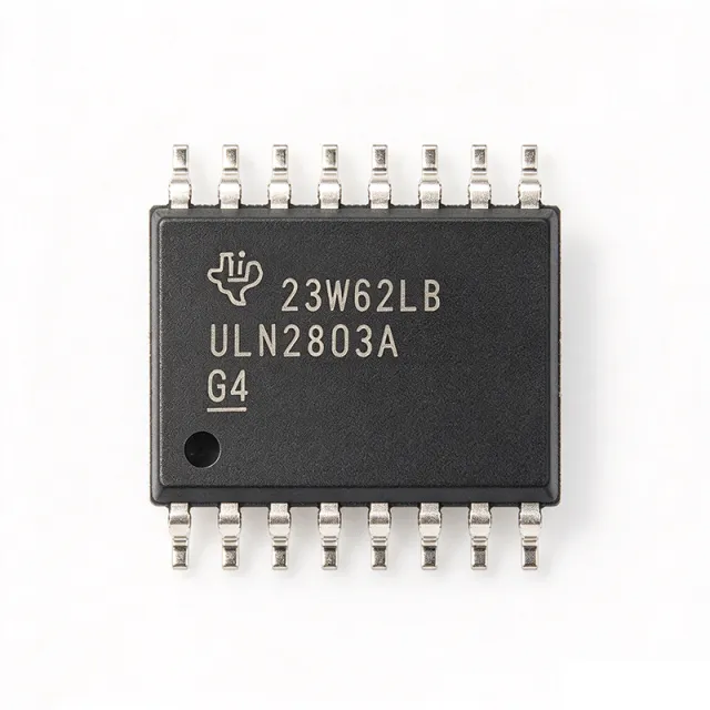
ULN2803ADWR - 8-Channel 50V 500mA Darlington Array | TI
The Texas Instruments ULN2803ADWR is a high-voltage, high-current Darlington transistor array integrating eight NPN Darlington pairs into a single 18-pin SOIC (DW) surface-mount package, each rated 50 V collector-emitter and 500 mA collector current. The device features integrated common-cathode clamp diodes tied to a dedicated COM pin (pin 10) for switching inductive loads such as relays and solenoids. Logic inputs are TTL/5 V CMOS compatible via on-chip 2.7 kOhm base resistors, and channels may be paralleled for higher currents. A Darlington transistor array is an integrated circuit that combines multiple Darlington pairs - two bipolar transistors cascaded for very high current gain (hFE typically >1000) - into a single die. This category belongs to the power switch / load driver family within power-management semiconductors, sitting under the broader umbrella of discrete-array ICs. By integrating eight drivers, the part allows low-current logic outputs from microcontrollers, TTL, or CMOS gates to switch high-current loads with a minimum of external components. Key features include 50 V continuous collector-emitter rating, 500 mA continuous collector current per channel (with peak inrush capability higher due to Darlington dynamics), 2.7 kOhm input base resistors allowing direct interface to 3.3 V and 5 V logic, and built-in flyback clamp diodes tied to COM. The -40 C to +85 C operating temperature range covers industrial environments. The 18-SOIC (DW) footprint is JEDEC-standard and footprint-compatible with several legacy through-hole-to-SMD migration designs. Internally, each Darlington pair includes base and emitter resistors that set predictable turn-on thresholds and stabilize off-state leakage, while the integrated clamp diodes provide a defined current path for inductive kickback. Total package dissipation is bounded by thermal resistance; at 25 C ambient with adequate PCB copper, approximately 1.4 W is achievable. Output saturation voltage of about 1 V at rated current is the typical Darlington trade-off for high gain. Typical applications include 5 V relay driver arrays, stepper motor winding drivers (commonly with bipolar stepper motors in 3D printers, CNC machines, and robotics), solenoid and valve drivers, LED and lamp matrix drivers, and logic-level buffers. The part directly interfaces MCU GPIO to high-current loads in a single SOIC-18 footprint, eliminating discrete transistor driver stages. Always connect the COM pin (pin 10) to the positive supply of the inductive load so the clamp diodes can absorb back-EMF. Budget total package dissipation across all active channels and use adequate copper pour. This device is in Last Time Buy - consider drop-in alternatives below for new designs. This page synthesizes distributor stock, drop-in alternatives, and practical design notes not consolidated in the manufacturer datasheet, helping engineers migrate from this LTB part with minimal PCB rework.

ULN2803APG - 8ch Darlington Sink Driver, 50V, 500mA DIP-18
The Toshiba ULN2803APG is an 8-channel high-voltage, high-current Darlington sink driver housed in a 18-pin DIP (through-hole) package. It integrates eight NPN Darlington pairs with integral clamp diodes for switching inductive loads, delivering up to 500 mA per channel and 50 V collector-emitter breakdown voltage. Each Darlington pair features a base-emitter input resistor of 2.7 kOhm, allowing direct CMOS/TTL logic interface at 5 V inputs. A Darlington transistor array is a monolithic bipolar IC that pairs two NPN transistors so the emitter of the first drives the base of the second, multiplying current gain (hFE typically > 1000). Eight such pairs share a common-emitter ground pin, forming an 8-channel low-side switch well suited to driving relays, solenoids, stepper motor windings, lamp filaments, and LED displays from low-power digital logic. The ULN2803 family sits within the broader hierarchy of bipolar transistor arrays → interface ICs → driver ICs → power management. Key specifications of the ULN2803APG include 500 mA continuous collector current per channel, 50 V VCEO sustain voltage, integrated free-wheeling clamp diodes on each output for inductive load protection, and an input structure compatible with 5 V CMOS logic levels. The DIP-18 footprint matches industry-standard pinouts used by competing parts from TI, STMicroelectronics, and Allegro, simplifying PCB migration. Typical applications span relay drivers in industrial control, hammer/lamp drivers in point-of-sale and copier equipment, LED/display matrix drivers, and stepper or DC motor bridge half-drivers. The integrated clamp diodes eliminate external snubbers on solenoids and relay coils, reducing BOM count and improving long-term reliability against back-EMF transients. When designing with this device, observe the package power dissipation limit of 760 mW for the DIP-18 variant and derate per channel when multiple outputs switch simultaneously at high duty cycle. The common-emitter architecture makes the ULN2803APG strictly a low-side (sink) driver — for high-side (source) driving use the complementary ULN2803 family high-side counterpart or a PNP/PMOS array.
ULN2803APG5M - 8ch 50V/500mA Darlington Sink Driver | Toshiba
The Toshiba ULN2803APG5M is a monolithic high-voltage, high-current Darlington transistor array comprising eight NPN Darlington pairs with integral clamp diodes for inductive-load switching. Each Darlington channel is rated to 50 V collector-emitter and 500 mA continuous collector current (760 mW total package dissipation), making it a true 8-channel open-collector sink driver in a 18-DIP through-hole package. The (5,M) suffix indicates 5-piece minimum order pack shipped from the Toshiba tube / tray manufacturing flow. A Darlington transistor array is a class of bipolar driver in which two transistors are cascaded (collector of the input transistor tied to the base of the output transistor) so that the input sees only the very small base current of the first device, while the output stage delivers the load current. The resulting current gain (hFE) of several thousand allows logic-level signals (5 V CMOS, 3.3 V TTL, or even microcontroller GPIO) to directly switch much higher currents and voltages. Within the broader taxonomy, the ULN2803APG5M belongs to the Bipolar Transistor Array (BJT array) family, sits inside the Power Management / Interface & Driver category, and ultimately functions as a low-side (sink) driver. The integral freewheeling clamp diodes across each output protect the IC when driving relays, solenoids, and motors from the inductive kick that would otherwise destroy the output transistors. Key differentiating features include eight parallel channels in one package (saving PCB area versus discrete transistors), 50 V rating that comfortably covers 24 V industrial and automotive relays, 500 mA continuous per channel (higher peaks possible within SOA limits), built-in input resistors for direct 5 V logic compatibility, and the 18-DIP through-hole footprint that remains the industry standard for breadboarding, legacy designs, and pin-compatible cross-brand substitutions. Compared with discrete MOSFETs, the Darlington array offers simpler drive and lower BOM cost but trades away switching speed, so it is best suited for slow on/off actuation rather than high-frequency PWM. The architecture uses eight common-emitter Darlington switches whose emitters are tied to a common ground pin, while each open collector is brought out separately to a DIP pin. The clamp diode anode connects to Vsup and cathode to each collector, suppressing flyback voltage transients. Total power dissipation of 760 mW for the package (about 95 mW per channel continuous) defines the safe envelope. Typical applications include 5 V logic-to-24 V relay driver boards, stepper motor phase drivers for small unipolar motors, solenoid and valve drivers, LED matrix row/column drivers, thermal printer head drivers, and lamp/indicator banks. When designing with this device, always verify package dissipation against the worst-case simultaneous-channel conduction: eight 100 mA outputs will exceed the 760 mW package rating unless derated.
ULN2803APGCNHZN - 8ch Darlington Sink Driver 50V/500mA DIP-18 | Toshiba
The Toshiba ULN2803APGCNHZN is an 8-channel high-voltage, high-current Darlington sink driver array housed in a 18-pin DIP package. Each of the eight NPN Darlington pairs can sink up to 500 mA continuously and is rated for 50 V collector-emitter voltage, with integral free-wheeling clamp diodes for switching inductive loads such as relays, solenoids, stepper motors and small DC loads. A Darlington transistor array is a type of bipolar junction transistor (BJT) driver that pairs two transistors in a Darlington configuration to multiply current gain (hFE), allowing a low-current logic signal (such as a 5 V TTL or 3.3 V CMOS microcontroller output) to switch high-current loads. Within the broader semiconductor taxonomy, the ULN2803 belongs to the power transistor array family, which sits under interface ICs and power management ICs used to bridge low-power digital controllers and high-power actuators. Eight such drivers are integrated into a single package, providing a compact, pin-efficient solution for multi-channel switching. Key features include 500 mA continuous collector current per channel, 50 V minimum collector-emitter breakdown voltage, integral clamp diodes for inductive load protection, TTL/CMOS-compatible inputs via the 2.7 kOhm base resistor network, and an 18-pin DIP (through-hole) package that simplifies prototyping and breadboard use. The 8-channel parallel architecture allows simultaneous control of multiple loads using a single IC, reducing BOM and PCB area. The device is fabricated using a bipolar junction transistor (BJT) process optimized for high-voltage, high-current switching. The monolithic silicon construction provides matched base resistors per channel, ensuring consistent drive behavior across all eight outputs, while the common-cathode clamp diodes tied to a dedicated COM pin simplify inductive load management. Typical applications include relay drivers, solenoid drivers, stepper motor unipolar winding drivers, LED matrix row/column drivers, lamp drivers, logic-level translators, and general-purpose high-current sink switching for industrial automation, consumer appliances, and HVAC controls. In microcontroller-based designs, the ULN2803 typically sits between a 5 V GPIO and a 24 V load bus. When designing with this part, ensure that the sum of all simultaneously-active channel currents does not exceed the package's total power dissipation of approximately 1.47 W, and always connect the COM pin to the positive supply when driving inductive loads so that the internal clamp diodes can recirculate the back-EMF. Avoid exceeding the 50 V VCEO rating, especially with inductive kick. This page synthesizes distributor pricing, drop-in same-package and cross-brand alternatives, and practical design notes not found in a single manufacturer datasheet, helping engineers shortlist a working part quickly.
ULN2803APGOM - 8CH 50V 500mA Darlington Sink Driver DIP-18 | Toshiba
The Toshiba ULN2803APGOM is an 8-channel high-voltage, high-current Darlington sink driver in an 18-pin PDIP (DIP-18) through-hole package. Each of the eight channels integrates an NPN Darlington pair rated at 50 V collector-emitter voltage and 500 mA continuous collector current, with integral free-wheeling clamp diodes for switching inductive loads such as relays, solenoids, and stepper motor windings. The CMOS-compatible 5 V logic inputs simplify direct connection to modern microcontrollers, and the (O,M) Toshiba marking suffix indicates factory-packaging/tray code rather than an electrical variant. A Darlington sink driver is a type of integrated bipolar transistor array that provides high current gain by cascading two NPN transistors inside a single package. The ULN2803APGOM belongs to the bipolar transistor array -> Darlington transistor array -> power management IC hierarchy. By sinking current to ground (low-side switching), it allows a low-power logic output to control high-power loads that would otherwise damage a microcontroller I/O pin. This topology is widely used for interface between digital control circuits and electromechanical actuators. Key specifications include a minimum DC current gain (hFE) of approximately 2000 at low collector current due to the Darlington cascade, an input series base resistor of 2.7 kOhm sized for 5 V CMOS logic, and an integral collector-emitter clamp diode on every channel rated for switching inductive transients. The package dissipates up to 2.25 W at 25 C ambient, derating linearly to zero at 125 C. The 18-pin PDIP form factor supports easy breadboarding and through-hole PCB prototyping. Typical applications include relay and solenoid drivers for industrial automation, unipolar stepper motor winding drivers, LED matrix row/column sinks, inkjet printer head drivers, and lamp/display drivers. The eight parallel channels also make it useful for multi-axis low-side switching in robotics and HVAC controls. When designing with this part, ensure that the total package dissipation does not exceed 2.25 W at 25 C ambient with appropriate linear derating above 25 C. Place flyback clamp diodes (already integrated) will protect the device when switching inductive loads, but external free-wheeling diodes or snubbers may be needed for very fast switching edges.

VIPERGAN65 - 650V GaN Power Transistor | STMicroelectronics
The STMicroelectronics VIPERGAN65 is a 650V enhancement-mode Gallium Nitride (GaN) power transistor designed for high-efficiency power conversion applications. It integrates a GaN power HEMT with a gate driver and protection features in a compact PQFN 8x8 mm package, enabling high-frequency operation and reduced system size. What is a GaN power transistor? A Gallium Nitride (GaN) power transistor is a wide-bandgap semiconductor device that switches faster and more efficiently than traditional silicon MOSFETs. It belongs to the power transistor family, which includes MOSFETs, IGBTs, and bipolar transistors. GaN devices offer lower on-resistance and lower gate charge, making them ideal for high-frequency power converters such as AC-DC adapters, server power supplies, and wireless charging systems. Key features of the VIPERGAN65 include a 650V drain-source voltage rating, low on-resistance (RDS(on)) of [DATA_NEEDED: RDS(on)], and a gate driver with integrated protection. The device supports high switching frequencies up to [DATA_NEEDED: max switching frequency] MHz, reducing the size of magnetic components. It also features overcurrent, overtemperature, and undervoltage lockout protection, enhancing system reliability. Technically, the VIPERGAN65 uses a cascode configuration with a GaN HEMT and a silicon MOSFET, simplifying gate drive requirements. The integrated driver eliminates external gate driver components, reducing board space and design complexity. The device's fast switching transitions minimize switching losses, improving overall efficiency in power conversion. Typical applications include AC-DC adapters for laptops and smartphones, server power supplies, and LED lighting drivers. The high efficiency and small form factor make it suitable for space-constrained designs. In a 65W USB-PD adapter, the VIPERGAN65 can achieve over 93% efficiency, reducing heat dissipation and enabling compact enclosures. When designing with the VIPERGAN65, ensure proper PCB layout with short, low-inductance paths for the gate drive and power loops. Use a dedicated ground plane and place decoupling capacitors close to the device. Thermal management is critical; use a thermal pad and adequate copper area to dissipate heat from the package.

VO1263AACTR - Dual Photovoltaic MOSFET Driver | Vishay
The Vishay VO1263AACTR is a dual-channel photovoltaic MOSFET driver optoisolator that delivers 9.8 V open-circuit output and 14 uA short-circuit current per channel from a 5 mA LED input, packaged in an 8-SMD (gull-wing) surface-mount form factor with 5300 Vrms input-to-output isolation. Each of the two independent channels contains a GaAlAs infrared LED optically coupled to a photodiode array that functions as a floating voltage source, providing the bias and turn-on energy required to drive the gate of a high-power MOSFET or IGBT in solid-state relay (SSR) and galvanically-isolated switching applications. A photovoltaic MOSFET driver (also called an optically-isolated gate driver or photovoltaic isolator) is a type of solid-state isolator that replaces the secondary-side bias supply and pulse transformer used in conventional isolated gate-drive circuits. The device sits in the signal chain between a low-voltage MCU/control IC and the gate of a high-voltage power switch, providing reinforced galvanic isolation while sourcing just enough current to charge the MOSFET gate to its threshold voltage. In the broader taxonomy it belongs to optocouplers -> isolators -> discrete semiconductors -> semiconductor devices, and is the modern descendant of the electromechanical relay in compact, long-lifetime switching. Key features include a low typical input forward current of 5 mA (IF), an open-circuit photovoltaic output voltage of 9.8 V (VOC), and a short-circuit current of 14 uA (ISC) at IF = 5 mA per channel. The device offers two independent channels in one package, a 5300 Vrms I/O isolation rating per Vishay's test methodology, and a -40C to +100C operating temperature range suitable for industrial and instrumentation environments. The 8-SMD gull-wing package supports standard surface-mount assembly and automated pick-and-place. Architecturally, the VO1263AACTR uses two matched GaAlAs infrared emitters whose output is sensed by two series-stacked photodiode arrays; the resulting photovoltaic stack delivers a stable floating source that can swing to several volts above the MOSFET source. An external gate-to-source resistor is required to define the off-state and to discharge the gate when the LED is turned off. Because the photovoltaic output is essentially a current source limited by the LED drive, switching speeds are modest (turn-on and turn-off in the millisecond range), which is acceptable for SSR contactor, analog-switch, and slow PWM applications. Typical applications include solid-state relays (AC and DC output variants), isolated analog switch multiplexers, floating MOSFET/IGBT gate drivers in industrial control, medical patient-isolation switching, and telecom line-card replacements for electromechanical relays. Designers choose this part when they need two isolated drive channels in one package without the complexity of a separate isolated bias supply. The main design consideration when using the VO1263AACTR is that the photovoltaic output is a current-limited floating source, so the external MOSFET must be selected so that its total gate charge QG can be supplied within the application's required turn-on time (QG must be less than ISC * t_on). Designers should also place a gate-to-source resistor (typically 100 kohm to 1 Mohm) close to the MOSFET gate to guarantee a defined off-state. This page synthesizes Vishay datasheet parameters, drop-in alternative cross-references, and practical SSRs/isolated gate-drive design notes not found on the manufacturer's product page alone.