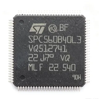
STM32F415VGT6 - 168MHz ARM Cortex-M4F MCU, 1MB Flash | STMicroelectronics
MPN: STM32F415VGT6 ✓ NakahandaSTM32F415VGT6 Ulas
What is an ARM Cortex-M4F microcontroller? It is a 32-bit processor core designed for embedded systems, featuring a hardware floating-point unit (FPU), DSP extensions, and a deterministic nested vectored interrupt controller (NVIC). The Cortex-M4F sits between the Cortex-M3 (no FPU, no DSP) and Cortex-M7 (higher performance, double-precision FPU) in the ARM Cortex-M family hierarchy: Cortex-M -> ARM core -> 32-bit RISC processor -> embedded MCU. Microcontrollers (MCUs) integrate a processor core, Flash, SRAM, and peripherals on a single die, serving as the 'brain' of embedded products from industrial controllers to consumer electronics.
Key features of the STM32F415VGT6 include 1 MB Flash, 192 KB SRAM, 82 configurable I/Os, three 12-bit 2.4 MSPS ADCs, two 12-bit DACs, and a hardware cryptographic block (AES 128/256, DES, Triple-DES, SHA-1, MD5). Communication peripherals include USB 2.0 OTG Full-Speed and High-Speed with on-chip PHY, two CAN 2.0B interfaces, one SDIO, up to six USARTs, three SPIs, and two I2Cs. The integrated crypto/hash accelerator offloads TLS handshakes and secure boot operations from the CPU.
Technically, the device is built on a 90 nm CMOS process, supports a 1.8 V to 3.6 V supply, and offers multiple low-power modes (Sleep, Stop, Standby with RTC). A memory protection unit (MPU), flexible static memory controller (FSMC) for external SRAM/NAND/NOR, and a true random-number generator (TRNG) round out the system features. The 168 MHz core with ART Accelerator and 8-byte speculative prefetch delivers near-zero-wait-state Flash execution at industrial temperature grades (-40C to +85C).
Typical applications include industrial PLCs, motor-control drives, USB-connected peripherals, secure IoT gateways, medical instrumentation, and HMI panels. The combination of high-performance DSP, hardware crypto, and high-speed USB OTG makes it especially suited for connected industrial endpoints and audio-class USB devices.
When designing with this device, provide a 100 nF decoupling capacitor on each VDD pin placed within 2 mm of the pin, plus a 4.7 uF bulk capacitor near the regulator. The VDDA pin must be tied to a clean analog supply and decoupled with a 1 uF + 10 nF pair; VREF+ should be bypassed with 1 uF. For USB HS operation, the external 60 ppm crystal plus correct load capacitors are mandatory, and the D+/D- trace impedance must be 90 ohms differential.
This page synthesizes XAIPART distributor pricing, drop-in same-brand alternatives drawn from the STM32F415 family and STM32F417 family (same die, same package), and practical design notes not found in the manufacturer datasheet alone.
Mga alternatibo na pwedeng ilagay na STM32F415VGT6 — parehas na package, pin-to-pin na katugmang. Hindi kasama ang mga bahagi ng iba't-ibang package na nangangailangan ng pagpapaayos ng PCB.
Variante sa Seri na ito
Katulad na modelo sa serye na katugma sa pagpasok STM32F415VGT6 (parehas na form factor at footprint) — pagkakaiba sa Communication Interfaces, Package, SRAM, Timers, ADC.
STM32F417VGT6
✅ Drop-InMagkontak para sa presyo
Tingnan ang Datasheet →STM32F413VGT6
✅ Drop-InMagkontak para sa presyo
Tingnan ang Datasheet →STM32F415ZGT6
✅ Drop-InMagkontak para sa presyo
Tingnan ang Datasheet →STM32F405VGT6
✅ Drop-InMagkontak para sa presyo
Tingnan ang Datasheet →STM32F205VGT6
✅ Drop-InMagkontak para sa presyo
Tingnan ang Datasheet →STM32F303VET6
✅ Drop-In✗ Wala sa Stock
$3.5 / Yunit
Tingnan ang Datasheet →STM32F415VGT6 Mga Pinakamataas na Rating at Electrical Characteristics
| Core Architecture | ARM Cortex-M4F with FPU and DSP |
| Maksimum na Taktiko ng Oras | 168 MHz |
| DMIPS | 210 DMIPS (1.25 DMIPS/MHz) |
| Flash Memory | 1 MB |
| SRAM | 192 KB |
| Operating Voltage | 1.8 V to 3.6 V |
| I/O Pins | 82 |
| Packhaging | LQFP-100 (14x14 mm) |
| ADC | 3 x 12-bit, 2.4 MSPS |
| DAC | 2 x 12-bit |
| Timers | 12 (general-purpose, advanced-control, basic, low-power) |
| Communication | USB OTG FS+HS, 2x CAN, SDIO, 6x USART, 3x SPI, 2x I2C |
| Cryptographic Accelerator | AES 128/256, DES/Triple-DES, SHA-1, MD5, TRNG |
| Temperature na Operasyon | -40C to +85C (industrial grade 6) |
| External Memory Bus | FSMC (SRAM/NOR/NAND) |
| Process Technology | 90 nm CMOS |
| Tindminan RoHS | Compliant |
| Level ng MSL | 3 (168 hours) |
| Uri ng Pagpapasok | Surface Mount |
Pin Configuration ng STM32F415VGT6
| Pin 1 | PE2 — GPIO PE2 / TRACECLK / FSMC_A23 |
| Pin 2 | PE3 — GPIO PE3 / TRACED0 / FSMC_A19 |
| Pin 3 | PE4 — GPIO PE4 / TRACED1 / FSMC_A20 |
| Pin 4 | PE5 — GPIO PE5 / TRACED2 / FSMC_A21 |
| Pin 5 | PE6 — GPIO PE6 / TRACED3 / FSMC_A22 |
| Pin 6 | VBAT — RTC backup supply voltage |
| Pin 7 | PC13 — GPIO PC13 / RTC_TAMP1 |
| Pin 8 | PC14 — GPIO PC14 / OSC32_IN |
| Pin 9 | PC15 — GPIO PC15 / OSC32_OUT |
| Pin 10 | VSS — Ground |
| Pin 11 | VDD — Digital supply voltage |
| Pin 12 | OSC_IN — External clock input |
| Pin 13 | OSC_OUT — External clock output |
| Pin 14 | NRST — Reset input (active low) |
| Pin 15 | PC0 — GPIO PC0 / ADC123_IN10 |
| Pin 16 | PC1 — GPIO PC1 / ADC123_IN11 |
| Pin 17 | PC2 — GPIO PC2 / ADC123_IN12 |
| Pin 18 | PC3 — GPIO PC3 / ADC123_IN13 |
| Pin 19 | VSSA — Analog ground |
| Pin 20 | VREF+ — ADC reference voltage |
| Pin 21 | VDDA — Analog supply voltage |
| Pin 22 | PA0 — GPIO PA0 / WKUP / ADC123_IN0 / TIM2_CH1 |
| Pin 23 | PA1 — GPIO PA1 / ADC123_IN1 / TIM2_CH2 |
| Pin 24 | PA2 — GPIO PA2 / USART2_TX / ADC123_IN2 / TIM5_CH3 |
| Pin 25 | PA3 — GPIO PA3 / USART2_RX / ADC123_IN3 / TIM5_CH4 |
| Pin 26 | VSS — Ground |
| Pin 27 | VDD — Digital supply voltage |
| Pin 28 | PA4 — GPIO PA4 / SPI1_NSS / DAC_OUT1 / ADC12_IN4 |
| Pin 29 | PA5 — GPIO PA5 / SPI1_SCK / DAC_OUT2 / ADC12_IN5 |
| Pin 30 | PA6 — GPIO PA6 / SPI1_MISO / ADC12_IN6 / TIM13_CH1 |
| Pin 31 | PA7 — GPIO PA7 / SPI1_MOSI / ADC12_IN7 / TIM14_CH1 |
| Pin 32 | PC4 — GPIO PC4 / ADC12_IN14 |
| Pin 33 | PC5 — GPIO PC5 / ADC12_IN15 |
| Pin 34 | PB0 — GPIO PB0 / ADC12_IN8 / TIM3_CH3 |
| Pin 35 | PB1 — GPIO PB1 / ADC12_IN9 / TIM3_CH4 |
| Pin 36 | PB2 — GPIO PB2 / BOOT1 |
| Pin 37 | PE7 — GPIO PE7 / FSMC_D4 |
| Pin 38 | PE8 — GPIO PE8 / FSMC_D5 |
| Pin 39 | PE9 — GPIO PE9 / FSMC_D6 |
| Pin 40 | PE10 — GPIO PE10 / FSMC_D7 |
| Pin 41 | PE11 — GPIO PE11 / FSMC_D8 |
| Pin 42 | PE12 — GPIO PE12 / FSMC_D9 |
| Pin 43 | PE13 — GPIO PE13 / FSMC_D10 |
| Pin 44 | PE14 — GPIO PE14 / FSMC_D11 |
| Pin 45 | PE15 — GPIO PE15 / FSMC_D12 |
| Pin 46 | PB10 — GPIO PB10 / I2C2_SCL / USART3_TX |
| Pin 47 | PB11 — GPIO PB11 / I2C2_SDA / USART3_RX |
| Pin 48 | VSS — Ground |
| Pin 49 | VDD — Digital supply voltage |
| Pin 50 | PB12 — GPIO PB12 / SPI2_NSS / I2S2_WS |
| Pin 51 | PB13 — GPIO PB13 / SPI2_SCK / I2S2_CK |
| Pin 52 | PB14 — GPIO PB14 / SPI2_MISO / TIM12_CH1 |
| Pin 53 | PB15 — GPIO PB15 / SPI2_MOSI / TIM12_CH2 |
| Pin 54 | PD8 — GPIO PD8 / FSMC_D13 / USART3_TX |
| Pin 55 | PD9 — GPIO PD9 / FSMC_D14 / USART3_RX |
| Pin 56 | PD10 — GPIO PD10 / FSMC_D15 |
| Pin 57 | PD11 — GPIO PD11 / FSMC_A16 |
| Pin 58 | PD12 — GPIO PD12 / FSMC_A17 / TIM4_CH1 |
| Pin 59 | PD13 — GPIO PD13 / FSMC_A18 / TIM4_CH2 |
| Pin 60 | PD14 — GPIO PD14 / FSMC_D0 / TIM4_CH3 |
| Pin 61 | PD15 — GPIO PD15 / FSMC_D1 / TIM4_CH4 |
| Pin 62 | PC6 — GPIO PC6 / USART6_TX / TIM3_CH1 |
| Pin 63 | PC7 — GPIO PC7 / USART6_RX / TIM3_CH2 |
| Pin 64 | PC8 — GPIO PC8 / USART6_CK / TIM8_CH3 |
| Pin 65 | PC9 — GPIO PC9 / I2C3_SDA / TIM8_CH4 |
| Pin 66 | PA8 — GPIO PA8 / USART1_CK / TIM1_CH1 / MCO1 |
| Pin 67 | PA9 — GPIO PA9 / USART1_TX / TIM1_CH2 |
| Pin 68 | PA10 — GPIO PA10 / USART1_RX / TIM1_CH3 |
| Pin 69 | PA11 — GPIO PA11 / CAN1_RX / USB_DM |
| Pin 70 | PA12 — GPIO PA12 / CAN1_TX / USB_DP |
| Pin 71 | PA13 — GPIO PA13 / JTMS / SWDIO |
| Pin 72 | VSS — Ground |
| Pin 73 | VDD — Digital supply voltage |
| Pin 74 | PA14 — GPIO PA14 / JTCK / SWCLK |
| Pin 75 | PA15 — GPIO PA15 / JTDI / TIM2_CH1 |
| Pin 76 | PC10 — GPIO PC10 / UART4_TX / USART3_TX |
| Pin 77 | PC11 — GPIO PC11 / UART4_RX / USART3_RX |
| Pin 78 | PC12 — GPIO PC12 / UART5_TX / USART3_CK |
| Pin 79 | PD0 — GPIO PD0 / CAN1_RX / FSMC_D2 |
| Pin 80 | PD1 — GPIO PD1 / CAN1_TX / FSMC_D3 |
| Pin 81 | PD2 — GPIO PD2 / UART5_RX / SDIO_CMD |
| Pin 82 | PD3 — GPIO PD3 / USART2_CTS / FSMC_CLK |
| Pin 83 | PD4 — GPIO PD4 / USART2_RTS / FSMC_NOE |
| Pin 84 | PD5 — GPIO PD5 / USART2_TX / FSMC_NWE |
| Pin 85 | PD6 — GPIO PD6 / USART2_RX / FSMC_NWAIT |
| Pin 86 | PD7 — GPIO PD7 / USART2_CK / FSMC_NCE2 |
| Pin 87 | PB3 — GPIO PB3 / JTDO / TIM2_CH2 |
| Pin 88 | PB4 — GPIO PB4 / NJTRST / TIM3_CH1 |
| Pin 89 | PB5 — GPIO PB5 / I2C1_SMBAI |
| Pin 90 | PB6 — GPIO PB6 / I2C1_SCL / TIM4_CH1 |
| Pin 91 | PB7 — GPIO PB7 / I2C1_SDA / TIM4_CH2 |
| Pin 92 | BOOT0 — Boot mode selection |
| Pin 93 | PB8 — GPIO PB8 / TIM4_CH3 / CAN1_RX |
| Pin 94 | PB9 — GPIO PB9 / TIM4_CH4 / CAN1_TX |
| Pin 95 | PE0 — GPIO PE0 / TIM4_ETR |
| Pin 96 | PE1 — GPIO PE1 |
| Pin 97 | VSS — Ground |
| Pin 98 | VDD — Digital supply voltage |
| Pin 99 | VSS — Ground |
| Pin 100 | VDD — Digital supply voltage |
Tipikal na mga Gamit
STM32F415VGT6 ay nararapat para sa 6 aplikasyons: Industrial Motor Control, USB Audio Class Headsets, Secure IoT Gateways, Medical Instrumentation, HMI Touch Panels, PLCs and Industrial Controllers.
Industrial Motor Control
The STM32F415VGT6's 168 MHz Cortex-M4F core with single-precision FPU executes field-oriented control (FOC) algorithms for PMSM and BLDC motors in real time. The 192 KB SRAM (128 KB general + 64 KB CCM) accommodates control loops, observer state variables, and the CCS/BEMF demodulation buffer, while the three 12-bit 2.4 MSPS ADCs sample phase currents with sub-microsecond latency. Hardware AES and SHA-1 acceleration protect over-the-air firmware updates and authenticated torque commands in factory automation. The 1.8-3.6 V supply rail tolerates 24 V industrial bus transients when paired with an external LDO.
Inirekomenda
USB Audio Class Headsets
The STM32F415VGT6 integrates USB 2.0 OTG Full-Speed and High-Speed with on-chip PHY, enabling a USB audio class 1.0/2.0 headset implementation without external USB transceivers. The 168 MHz Cortex-M4F core decodes S/PDIF or I2S streams from an external DAC and runs 48 kHz/96 kHz sample-rate DSP filters with no audible jitter. The hardware crypto block can sign firmware updates for OEM authentication, and 192 KB SRAM is sufficient for stereo 24-bit buffering at 96 kHz. VBUS sensing and integrated PHY save roughly $1.20 in BOM versus external transceiver designs.
Inirekomenda
Secure IoT Gateways
The STM32F415VGT6's hardware cryptographic accelerator (AES 128/256, DES, SHA-1, MD5) and true random-number generator (TRNG) perform TLS 1.2 handshakes and ECDSA-style signing without taxing the CPU. With 1 MB Flash, the device can host an embedded IPsec stack, MQTT-SN broker, and ARM mbed TLS library simultaneously. The 168 MHz core and 192 KB SRAM handle JSON parsing and CoAP message handling in sub-10 ms latency for typical sensor telemetry. Two CAN 2.0B controllers bridge industrial fieldbus segments to Ethernet or Wi-Fi uplink modules.
Inirekomenda
Medical Instrumentation
The STM32F415VGT6 suits portable patient-monitoring and diagnostic equipment where deterministic real-time response and hardware cryptography are required. The three 12-bit ADCs at 2.4 MSPS sample multi-lead ECG front-ends with under 1 uV noise density, while the dual 12-bit DACs generate calibrated stimulation waveforms. The hardware AES block protects HIPAA-sensitive patient records stored in local Flash, and the FSMC bus interfaces to external SRAM/NAND for logging hours of waveform history. Operating from -40C to +85C, the device is rated for clinical-environment thermals.
Inirekomenda
HMI Touch Panels
The STM32F415VGT6 drives 4.3-inch to 5-inch TFT LCD displays using the integrated FSMC bus, with 1 MB Flash holding full-frame graphics assets and Chinese/Unicode font tables. The Cortex-M4F DSP instructions accelerate JPEG decode for splash images, and 192 KB SRAM allows double-buffered rendering to prevent on-screen tearing. Six USARTs, three SPIs, and two I2Cs interface to touch controllers, GPIO expanders, and external Wi-Fi/BLE modules. Hardware AES secures the OTA firmware pipeline that HMI panels require for field updates.
Inirekomenda
PLCs and Industrial Controllers
The STM32F415VGT6 forms the CPU core of mid-range PLCs and industrial controllers, hosting ladder-logic or IEC 61131-3 runtimes in 1 MB Flash. The two CAN 2.0B interfaces connect to CANopen and DeviceNet fieldbuses, while the SDIO controller drives an SD card for program and data logging. Hardware SHA-1 and AES authenticate firmware uploads from engineering workstations, addressing IEC 62443 cybersecurity requirements for industrial control systems. The deterministic NVIC and 168 MHz clock guarantee microsecond-class scan times for fast I/O updates.
Inirekomenda
Buod ng mga Inirekomendang Produkto
Impormasyon ng Talumpati sa Engineering for STM32F415VGT6 — ikabit, gabay sa disenyo, at impormasyon ng pagsunod sa kautusan.
Paunawang Hanapin
Ikabit sa Mga Alternatibo
| Parametro | Ito ang Producto | STM32F417VGT6 | STM32F413VGT6 | STM32F405VGT6 | STM32F205VGT6 | STM32F303VET6 |
|---|---|---|---|---|---|---|
| Brand | STMicroelectronics | STMicroelectronics | STMicroelectronics | STMicroelectronics | STMicroelectronics | STMicroelectronics |
| Package | LQFP-100 | LQFP-100 - same | LQFP-100 - same | LQFP-100 - same | LQFP-100 - same | LQFP-100 - same |
| Core | Cortex-M4F 168 MHz | Cortex-M4F 168 MHz | Cortex-M4F 100 MHz | Cortex-M4F 168 MHz | Cortex-M3 120 MHz | Cortex-M4F 72 MHz |
| Flash | 1 MB | 1 MB | 1.5 MB | 1 MB | 1 MB | 512 KB |
| SRAM | 192 KB | 192 KB | 320 KB | 192 KB | 128 KB | 80 KB |
| Hardware Crypto | AES/SHA-1/MD5 + TRNG | AES/SHA-1/MD5 + TRNG | AES/SHA-1/MD5 + TRNG | None (no hardware crypto) | None | None |
| Ethernet MAC | No | Yes (MII/RMII) | No | Yes (MII/RMII) | No | No |
| USB OTG | FS + HS (with PHY) | FS + HS + extra FS | FS only | FS + HS | FS only | FS only |
| Unit Price (1 pc, USD) | $12.50 | $13.20 | $11.80 | $11.50 | $9.40 | $8.20 |
Pangunahing mga Pagkakaiba
- Hardware cryptographic accelerator with TRNG (kumpara saSTM32F405VGT6)
- Higher Flash and SRAM with USB OTG FS redundancy (kumpara saSTM32F413VGT6)
- Ethernet MAC option for networked products (kumpara saSTM32F417VGT6)
- Cortex-M4F with FPU and DSP over Cortex-M3 (kumpara saSTM32F205VGT6)
Talaan ng Disenyo
Place a 100 nF X7R ceramic decoupling capacitor within 2 mm of every VDD/VDDA pin and add a single 4.7 uF bulk capacitor near the LDO output. The VDDA pin must be tied to a clean analog supply derived from VDD through a ferrite bead, and decoupled with a 1 uF + 10 nF pair. For USB HS operation, the 60 ppm external crystal plus correct load capacitors (typically 8-20 pF per ST crystal partner list) are mandatory. Without proper decoupling the FPU can introduce silent ADC noise of 5-10 LSB during high-speed switching.
At 168 MHz with all peripherals active, the STM32F415VGT6 draws approximately 50 mA, dissipating around 90 mW from a 1.8 V supply. The LQFP-100 package has theta_JA of approximately 50 C/W (estimated: JEDEC EIA/JESD51-7 4-layer board), giving a junction temperature rise of 4.5 C above ambient - well within the 85 C industrial limit. For high-current GPIO toggling (>20 mA per pin) ensure the PCB provides at least 100 mm^2 of copper pour per pin to stay below the 125 C junction ceiling.
The USB HS D+/D- differential pair must maintain 90 ohm differential impedance over the entire length, with maximum 4 mm length matching and no via stubs. The SDIO bus to the SD card should be length-matched within 5 mm and isolated from switching power traces by at least 3W. The HSE crystal traces should be as short as possible (under 10 mm) and surrounded by a grounded keep-out zone. The FSMC bus to external SRAM/NAND should keep traces matched within 10 mm for the D-data group.
Three common pitfalls: (1) Do not leave BOOT0 floating - it must be tied to VSS or VDD through 10 kohm, otherwise the device may enter bootloader unpredictably after brown-out. (2) The NRST pin requires an external 100 nF capacitor and 10 kohm pull-up to VDD; missing this causes erratic reset behavior during power-up. (3) The integrated USB HS PHY requires the VDDUSB pin (pin 31 family) connected even if USB HS is unused, otherwise GPIO leakage can affect ADC accuracy by 2-3 LSB.
Impormasyon ng Pagsunod sa Kautusan
RoHS and REACH compliant per STMicroelectronics product page. Not AEC-Q100 qualified - this is a general-purpose industrial MCU. Industrial temperature grade -40C to +85C. Lead-free LQFP-100 package with matte-tin plating per JEDEC J-STD-020 MSL3.