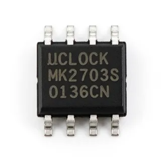
ICS551M - 1:4 160MHz CMOS Clock Buffer | Renesas
MPN: ICS551M ✗ Cuối đờiICS551M Tóm tắt
A clock fanout buffer is a clock-and-timing integrated circuit that distributes one incoming clock signal to multiple downstream loads. Its place in the hierarchy is clock buffer → clock fanout buffer → clock distribution IC → timing and logic semiconductor. The ICS551M helps isolate clock loads from one another, reduces loading on the source clock, and provides separate outputs for multiple sequential or peripheral circuits. This is especially useful when a single oscillator or clock source must feed several logic blocks.
Key verified characteristics include a 1:4 fanout ratio, 160 MHz maximum frequency, CMOS input and output technology, and an operating supply range of 3 V to 5.5 V. The 8-SOIC package measures 0.154 inches, or 3.90 mm, in width according to distributor data. These specifications make the device appropriate for general-purpose clock distribution where a compact surface-mount package and moderate operating frequency are sufficient.
The ICS551M belongs to the ICS ClockBlocks family and is identified by distributor listings as a low-cost, small clock buffer. Because its outputs are CMOS, the downstream circuits must be compatible with the selected supply voltage and input thresholds. The device is not a PLL, oscillator, or level shifter; its function is specifically clock replication and distribution. Designers should preserve the input and output timing relationship, maintain the required supply decoupling, and account for trace and load differences among the four outputs.
Typical applications include clock distribution in embedded control systems, digital logic networks, communications equipment, test and measurement systems, and general-purpose processor or peripheral clocking. For a design that needs more independent clock domains, frequency generation, or differential clock outputs, a different clock-and-timing device may be more appropriate. For applications requiring only one input and four CMOS copies, the ICS551M provides a straightforward distribution function in an established 8-SOIC footprint.
The main design consideration is ensuring that every connected load, trace, and voltage domain is compatible with the available 160 MHz clock. Check rise and fall-time requirements, fanout loading, power-supply noise sensitivity, and the clock-source timing margin before production release. This page synthesizes verified distributor specifications, sourcing links, package information, and engineering guidance while leaving unverified values explicitly unresolved.
The ICS551M datasheet and application information should be consulted for complete pin functions, electrical limits, timing characteristics, and recommended circuit implementation. Distributor data confirms the core identity and major specifications, but it does not provide enough evidence here to infer undocumented timing, current, or package dimensions.
Bộ thay thế dễ dàng lắp đặt cho ICS551M — cùng gói, chân-to-chân tương thích. Các bộ phận yêu cầu hàn PCB bị loại trừ.
Các biến thể trong loạt này
Các mẫu cùng loạt có thể lắp đặt dễ dàng tương thích với ICS551M (cùng hình factor và footprint) — khác nhau ở Package, Maximum Frequency, Supply Voltage Range, Device Type, Number of Outputs.
[DATA_NEEDED: verified same-package alternative 1]
✅ Drop-In📋 Tham chiếu thay thế (không có trong danh mục)
[DATA_NEEDED: verified same-package alternative 2]
✅ Drop-In📋 Tham chiếu thay thế (không có trong danh mục)
[DATA_NEEDED: verified same-package alternative 3]
✅ Drop-In📋 Tham chiếu thay thế (không có trong danh mục)
[DATA_NEEDED: verified same-package alternative 4]
✅ Drop-In📋 Tham chiếu thay thế (không có trong danh mục)
[DATA_NEEDED: verified same-package alternative 5]
✅ Drop-In📋 Tham chiếu thay thế (không có trong danh mục)
ICS551M Thông số kỹ thuật
| Product Type | Clock Fanout Buffer (Distribution) IC |
| Fanout Ratio | 1:4 |
| Maximum Frequency | 160 MHz |
| Input Technology | CMOS |
| Output Technology | CMOS |
| Supply Voltage Range | 3 V to 5.5 V |
| Số lượng đầu ra | 4 |
| Number of Inputs | 1 |
| Hộp | 8-SOIC |
| Package Width | 0.154 in (3.90 mm) |
| Kiểu lắp đặt | Surface Mount |
| Logic Family | CMOS |
| Chức năng | Single-input to four-output clock buffer |
| Product Family | ICS ClockBlocks |
Hướng dẫn cấu hình chân ICS551M 0.154 in (3.90 mm)
Cấu hình chân cho ICS551M (0.154 in (3.90 mm) gói). Số thứ tự chân, chức năng và sơ đồ kết nối được xác định trong tài liệu thông số kỹ thuật của nhà sản xuất. Tham khảo nó để biết footprint và hướng dẫn hàn chính xác.

Không có dữ liệu chân cụ thể sẵn có cho ICS551M.
Tham khảo: tài liệu kỹ thuật cho cấu hình chân đầy đủ.
Ứng dụng tiêu biểu
ICS551M phù hợp cho 6 Áp dụngs: Embedded Control Clock Distribution, Communications Equipment Clock Fanout, Digital Logic Clock Tree, Test and Measurement Clock Systems, Processor and Peripheral Clocking, Industrial Control and Automation Logic.
Embedded Control Clock Distribution
ICS551M fits embedded control designs that already have a stable CMOS master clock but need multiple independently routed copies. Its 1:4 fanout ratio lets one source feed four logic blocks without requiring a PLL or oscillator. The verified 160 MHz maximum frequency supports moderate-speed digital systems, while the 3 V to 5.5 V range allows operation across common supply levels. Place the buffer close to the clock source when trace lengths or branch loading are significant, and route each output toward its intended load. Confirm input and output timing limits from the complete datasheet before using the device on a high-speed control bus.
Được đề xuất
Communications Equipment Clock Fanout
ICS551M is appropriate for communications equipment that distributes a shared CMOS clock to multiple serial, interface, or control blocks. The four outputs help separate physical branches and reduce the electrical loading presented to the original clock source. Its 160 MHz verified ceiling provides margin for many moderate-speed digital subsystems, but the final timing budget still depends on the source waveform, trace delay, load capacitance, and receiving device requirements. Use short, well-routed clock traces and maintain a continuous ground reference. Because ICS551M is a fanout buffer rather than a jitter attenuator or PLL, retain a clean source clock and verify edge-rate requirements.
Được đề xuất
Digital Logic Clock Tree
ICS551M can serve as a dedicated clock-tree element when several CMOS logic sections need separate copies of one reference signal. The 1:4 ratio provides a simple topology in which four branches can feed counters, state machines, serial engines, or peripheral control blocks. With a verified 160 MHz maximum frequency and 3 V to 5.5 V supply range, it is suitable for general-purpose logic rather than ultrafast processor clocking. Keep the input edge rate within the manufacturer's limits, place decoupling close to the device, and avoid excessive fanout capacitance on one output. Validate setup and hold timing at every receiver, especially when clock and data paths have different lengths.
Được đề xuất
Test and Measurement Clock Systems
ICS551M may be used in test and measurement equipment to distribute a master reference clock to counters, capture logic, converters, or interface modules. The 1:4 architecture allows four measurement channels or timing domains to share a source without directly loading one another. The device's 160 MHz maximum frequency is useful for moderate-speed instrumentation, but measurement accuracy can still be affected by source jitter, edge rate, and trace skew. Use controlled impedance and matched routing when the clock is part of a precision timing path. The supplied verified data does not specify jitter, skew, or propagation-delay limits, so those values must be obtained from the manufacturer datasheet before precision timing use.
Được đề xuất
Processor and Peripheral Clocking
ICS551M is useful when a processor or peripheral subsystem requires several copies of one CMOS clock. The single input and four outputs create a simple distribution point for processor peripherals, memory-control logic, serial engines, and supervisory circuits. The verified 3 V to 5.5 V supply range helps align the buffer with common digital rails, while the 160 MHz ceiling accommodates many embedded and control-clock requirements. Designers should verify the source clock's rise and fall times, receiver thresholds, output loading, and maximum clock frequency at the actual voltage. Avoid assuming that a fanout buffer corrects jitter, changes frequency, or provides level translation; its verified role is clock replication.
Được đề xuất
Industrial Control and Automation Logic
ICS551M supports compact industrial control boards that distribute a common clock among sensor interfaces, sequencing logic, communication modules, and actuator-control circuits. Its 1:4 fanout is convenient for partitioning a clock tree across functional blocks, and the 8-SOIC package supports conventional surface-mount assembly. The verified maximum frequency of 160 MHz provides a clear upper design limit, while the 3 V to 5.5 V supply range supports common industrial logic rails when the downstream devices match. Keep clock routing away from noisy switching nodes, use a solid ground plane, and confirm that cable or sensor interfaces do not add excessive capacitive loading. Industrial temperature and EMC requirements must be checked separately because those ratings are not provided in the verified data.
Được đề xuất
Tóm tắt các sản phẩm được đề xuất
Dữ liệu tham khảo kỹ thuật cho ICS551M — so sánh, hướng dẫn thiết kế và thông tin tuân thủ.
Hướng dẫn chọn lựa
So sánh với các sản phẩm thay thế
| Tham số | Sản phẩm này | [DATA_NEEDED: verified same-package alternative 1] | [DATA_NEEDED: verified same-package alternative 2] | [DATA_NEEDED: verified same-package alternative 3] |
|---|---|---|---|---|
| Package | 8-SOIC | 8-SOIC | 8-SOIC | 8-SOIC |
| Brand | Renesas Electronics | Renesas Electronics | Renesas Electronics | Renesas Electronics |
Bảo phân biệt quan trọng
- Simple one-to-four CMOS clock distribution (vsICS552-01B)
- Compact 8-SOIC implementation (vsICS552-01B)
- Moderate-speed application coverage (vsHigher-frequency clock-buffer products)
Ghi chú thiết kế
Route the single input clock to the ICS551M input pin with a short, direct trace, then branch the four outputs toward their respective loads. Keep clock traces away from switching power nodes, high-current return paths, and noisy digital interfaces. Because the device is a fanout buffer rather than a PLL, preserving input edge quality is important. Confirm trace length and load capacitance against the complete manufacturer timing data before enabling high-frequency operation.
Use a bypass capacitor close to the supply connection and provide a low-impedance ground reference. The verified supply range is 3 V to 5.5 V, so downstream CMOS loads must be compatible with the selected rail. Do not assume that the buffer isolates power-supply noise; clock outputs can still be affected by supply disturbances. Check the datasheet for recommended capacitance, supply-current limits, and voltage sequencing before finalizing the power architecture.
Do not use ICS551M as a frequency generator, level shifter, or PLL. It requires an incoming CMOS clock and produces four CMOS copies, so the source frequency and edge rate must already satisfy the system requirements. Also avoid treating the 160 MHz listing as a guarantee of usable system frequency without checking propagation delay, output skew, loading, and receiver timing. These parameters were not present in the supplied verified data and must be obtained from the manufacturer datasheet.
Thông tin tuân thủ
The supplied verified web results identify the component, function, electrical basics, package, and distributor listing, but do not provide RoHS, REACH, lead-free, halogen-free, or conflict-minerals declarations. Compliance must be confirmed with Renesas or an authorized distributor. AEC-Q100 is not applicable based on the verified data.