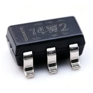
LMV321IDBVR - 1-MHz RRO Op Amp Single 5.5V | Texas Instruments
MPN: LMV321IDBVR ✓ Hoạt độngLMV321IDBVR Tóm tắt
A rail-to-rail output (RRO) op amp is a linear amplifier whose output voltage can swing to within tens of millivolts of either supply rail, maximizing dynamic range in low-voltage single-supply systems. Compared with general-purpose amplifiers that lose 1 V to 2 V of headroom on each side, an RRO part lets the designer use the full ADC input range on a 3.3 V or 5 V rail. The LMV321 belongs to the broader family of CMOS operational amplifiers, a category of analog ICs that trades the lower noise of bipolar parts for very low quiescent current and single-supply operation.
Key features include 1 MHz gain bandwidth product, 130 µA typical quiescent current, no output phase reversal, low crossover distortion, and an industry-standard 5-pin SOT-23 footprint. An internal ESD clamp and EMI filtering are characteristics of the larger LMV321A family; the original LMV321 line is recommended for cost-sensitive designs where these features are not required. The device is unity-gain stable and drives 2 kΩ loads comfortably at 5 V.
The LMV321 is built on a CMOS process with a differential input pair and a rail-to-rail class-AB output stage, which keeps crossover distortion low compared to single-ended class-A CMOS outputs. The PSRR is specified at 50 dB at 1 kHz, and the input common-mode range extends from the negative rail to within 1.2 V of the positive rail — adequate for single-supply sensor buffers and instrumentation front-ends.
Typical applications include single-supply sensor signal conditioning, current-sensing shunts in portable battery packs, low-side current monitors, headphone line drivers, and 5 V active filters. The part is widely used as a buffer/amplifier stage between photodiodes, thermistors, or strain gauges and downstream ADCs in IoT nodes.
When designing with this device, place a 1 nF to 10 nF decoupling capacitor within 2 mm of the VCC pin and keep input trace lengths short to limit leakage-induced offsets. For driving heavy loads or large capacitive loads, add a 50 Ω to 100 Ω series resistor at the output to prevent oscillation.
This page synthesizes distributor pricing, drop-in same-footprint alternatives, and practical design notes not found in the manufacturer datasheet.
Bộ thay thế dễ dàng lắp đặt cho LMV321IDBVR — cùng gói, chân-to-chân tương thích. Các bộ phận yêu cầu hàn PCB bị loại trừ.
Các biến thể trong loạt này
Các mẫu cùng loạt có thể lắp đặt dễ dàng tương thích với LMV321IDBVR (cùng hình factor và footprint) — khác nhau ở Number of Channels, Operating Temperature Range, Output Type, Input Type, Input Voltage Noise Density.
LMV321AIDBVR
✅ Drop-In📋 Tham chiếu thay thế (không có trong danh mục)
TLV3201AIDBVR
✅ Drop-In📋 Tham chiếu thay thế (không có trong danh mục)
TLV9061IDBVR
✅ Drop-In📋 Tham chiếu thay thế (không có trong danh mục)
TLV9041IDBVR
✅ Drop-In📋 Tham chiếu thay thế (không có trong danh mục)
TSV321IDBVR
✅ Drop-In📋 Tham chiếu thay thế (không có trong danh mục)
LMV321SN3T1G
✅ Drop-In📋 Tham chiếu thay thế (không có trong danh mục)
TP321-TR
✅ Drop-In📋 Tham chiếu thay thế (không có trong danh mục)
LMV321IDBVR Tỷ lệ tối đa & tính chất điện
| Number of Channels | 1 (Single) |
| Kiểu đầu ra | Rail-to-Rail |
| Gain Bandwidth Product (GBP) | 1 MHz |
| Supply Voltage (Single, 5V characterized) | 2.7 V to 5.5 V |
| Quiescent Current (typ) | 130 µA |
| Power Supply Rejection Ratio (PSRR) | 50 dB at 1 kHz (per family datasheet summary) |
| Khoảng nhiệt độ hoạt động | -40 °C to +125 °C |
| Hộp | SOT-23-5 (DBV) |
| Kiểu lắp đặt | Surface Mount |
| Cấp MSL | 1 (unlimited floor life, per JEDEC J-STD-020) |
| Trạng thái RoHS | Compliant |
| Lead-Free Finish | Yes (NiPdAu) |
Cấu hình chân LMV321IDBVR
| Chân 1 | OUT — Amplifier output (rail-to-rail) |
| Chân 2 | VCC- / IN- — Negative supply / inverting input (per LMV321 DBV pinout) |
| Chân 3 | IN+ — Non-inverting input |
| Chân 4 | VCC — Positive supply (2.7 V to 5.5 V) |
| Chân 5 | NC — Not connected (per datasheet pinout) |
Ứng dụng tiêu biểu
LMV321IDBVR phù hợp cho 6 Áp dụngs: Battery-Powered Sensor Signal Conditioning, Low-Side Current Sensing Amplifier, Headphone / Audio Line Driver, Photodiode Transimpedance Amplifier, Active Filter for ADC Anti-Aliasing, Industrial 4-20 mA Current Loop Transmitter.
Battery-Powered Sensor Signal Conditioning
The LMV321IDBVR is widely deployed as the front-end amplifier for low-frequency analog sensors (thermistor, strain gauge, pH probe, gas sensor) in coin-cell and 2 x AA battery products. Its 130 µA typical quiescent current adds negligible load to the cell while still delivering 1 MHz GBP — enough to buffer high-impedance sensor outputs without 1/f noise overwhelming the signal. The rail-to-rail output lets the next-stage ADC use the full 0 V to VCC input range, doubling usable dynamic range versus a non-RRO part on a 3.3 V rail. In a typical design, the LMV321 sits between a 10 kΩ Wheatstone bridge and a 12-bit SAR ADC running at 100 kSPS, with a 10 nF decoupling cap within 2 mm of the VCC pin.
Được đề xuất
Low-Side Current Sensing Amplifier
For battery management and motor-drive current monitoring, the LMV321IDBVR is used as a differential amplifier across a 10 mΩ to 100 mΩ shunt resistor. Its input common-mode range to the negative rail is essential because the shunt sits in series with the load return, which can be near ground or below ground during inductance ringing. The 1 MHz GBP introduces only ~5 µs of additional delay at 50 kHz PWM frequencies — adequate for sub-kHz current loops. Designers bias the non-inverting input to VCC/2 with a resistor divider to keep the output within the rail, and add a 50 Ω series output resistor if the load is capacitive.
Được đề xuất
Headphone / Audio Line Driver
Consumer headphone amplifiers and line-level audio outputs frequently use the LMV321IDBVR as a unity-gain buffer driving 16 Ω to 32 Ω earphones from a low-voltage DAC. Its rail-to-rail output swing maximizes the audio dynamic range on a 3.3 V or 5 V rail, while 1 MHz GBP comfortably covers the 20 Hz to 20 kHz audio band with low distortion. The 130 µA Iq keeps total idle current in the single-digit mW region, important for battery-powered Bluetooth headphones. A typical circuit adds an AC-coupling capacitor in series with the output and a 10 kΩ load to ground, with the part operating from VCC = 3.3 V.
Được đề xuất
Photodiode Transimpedance Amplifier
A single LMV321IDBVR can function as a low-cost transimpedance front-end for visible-light or IR photodiodes in smoke detectors, heart-rate monitors, or proximity sensors. The 1 MHz GBP and low input bias current (sub-pA with CMOS inputs) support feedback resistors up to ~1 MΩ without instability, giving sensitivities in the µA/nW range. Because the photodiode is biased near ground and the op-amp output sits near VCC/2, the rail-to-rail output stage keeps the diode in its linear region even on 3.3 V supplies. A 10 pF feedback capacitor in parallel with Rf prevents peaking, and the 5-pin SOT-23 footprint keeps the BOM cost below $0.20.
Được đề xuất
Active Filter for ADC Anti-Aliasing
The LMV321IDBVR works well as a Sallen-Key or multiple-feedback active low-pass filter for 3rd-order, 4th-order anti-aliasing stages ahead of sigma-delta ADCs in instrumentation and metering. With 1 MHz GBP, designers can realize filter corner frequencies up to ~50 kHz while maintaining at least 20 dB of gain margin at the unity-gain crossover. The rail-to-rail output stage allows the filter output to track the ADC's common-mode input, simplifying single-supply designs. A 4th-order Butterworth with fc = 10 kHz is a common recipe; placing a 10 nF to 100 nF capacitor across the feedback resistor tames peaking at the resonant frequency.
Được đề xuất
Industrial 4-20 mA Current Loop Transmitter
On the transmitter side of an industrial 4-20 mA current loop, the LMV321IDBVR can be used as the error amplifier inside the V-to-I converter that drives the loop. Its ability to operate from a single 5 V rail and stay within 2.7 V to 5.5 V across wide temperature ranges suits 24 V industrial loops after the local regulator drops to 5 V. The 130 µA Iq keeps the loop itself well above 4 mA at zero signal. A typical circuit uses the LMV321 with a 250 Ω sense resistor and a 2N3904 pass transistor, creating a stable 4 mA to 20 mA loop from a 0 V to 4 V DAC output.
Được đề xuất
Tóm tắt các sản phẩm được đề xuất
Dữ liệu tham khảo kỹ thuật cho LMV321IDBVR — so sánh, hướng dẫn thiết kế và thông tin tuân thủ.
Hướng dẫn chọn lựa
So sánh với các sản phẩm thay thế
| Tham số | Sản phẩm này | LMV321AIDBVR | TLV3201AIDBVR | TLV9061IDBVR | TSV321IDBVR | LMV321SN3T1G | TP321-TR |
|---|---|---|---|---|---|---|---|
| Brand | Texas Instruments | Texas Instruments | Texas Instruments | Texas Instruments | STMicroelectronics | onsemi | 3PEAK |
| Package | SOT-23-5 (DBV) | SOT-23-5 (DBV) — same | SOT-23-5 (DBV) — same | SOT-23-5 (DBV) — same | SOT-23-5 (DBV) — same | SOT-23-5 (DBV) — same | SOT-23-5 (DBV) — same |
| Channels | 1 (Single) | 1 (Single) | 1 (Single, comparator) | 1 (Single) | 1 (Single) | 1 (Single) | 1 (Single) |
| Supply Voltage Range | 2.7 V to 5.5 V | 2.7 V to 5.5 V | 2.7 V to 5.5 V | 1.8 V to 5.5 V (wider) | 2.5 V to 5.5 V | 2.7 V to 5.5 V | 2.5 V to 5.5 V |
| Gain Bandwidth Product | 1 MHz | 1 MHz | N/A (comparator; prop delay 40 ns) | 10 MHz | 1.4 MHz | 1 MHz | 1 MHz |
| Quiescent Current (typ) | 130 µA | 130 µA | 50 µA | 538 µA | 500 µA | 130 µA | 150 µA |
| Output Type | Rail-to-Rail Output | Rail-to-Rail Output | Open-Drain / Push-Pull comparator output | Rail-to-Rail I/O | Rail-to-Rail Output | Rail-to-Rail Output | Rail-to-Rail Output |
| Operating Temperature | -40 °C to +125 °C | -40 °C to +125 °C | -40 °C to +125 °C | -40 °C to +125 °C | -40 °C to +125 °C | -40 °C to +85 °C (commercial) | -40 °C to +125 °C |
| Approx. Unit Price (qty 1000) | $0.14 | $0.18 (est.) | $0.28 (est.) | $0.30 (est.) | $0.22 (est.) | $0.16 (est.) | $0.05 (est., China-domestic) |
Bảo phân biệt quan trọng
- Industry-benchmark cost / availability in SOT-23-5 (vsTLV9061IDBVR)
- Mature, broadly second-sourced design (vsTLV9041IDBVR)
- Higher bandwidth vs lower-Iq competitor (vsTSV321IDBVR)
Ghi chú thiết kế
Decouple VCC with a 0.1 µF ceramic capacitor placed within 2 mm of the supply pin, in parallel with a 1 µF to 10 µF bulk capacitor at the regulator output. The LMV321's 130 µA quiescent current is small enough that supply-line noise from a switching regulator can couple into the output — add an RC pi-filter (10 Ω + 10 µF) on the VCC rail if the part follows a noisy DC-DC converter. Estimated: power dissipation at 5 V is ~0.65 mW, well within SOT-23-5 thermal limits.
Route input traces away from noisy digital or switching signals; keep trace impedance below 100 Ω by using a ground plane on the input layer. For photodiode TIA applications, minimize the loop area of the feedback resistor and capacitor to limit stray capacitance — every extra pF of feedback capacitance reduces phase margin by roughly 1.5 ° per pF at the unity-gain crossover, and instability appears above ~5 pF with a 1 MΩ Rf.
The CMOS input stage has very low bias current but is sensitive to ESD; if the input will be exposed to user-accessible connectors, add a TVS diode and a 10 kΩ to 100 kΩ series resistor. The LMV321A variant integrates internal RFI/EMI filtering and 4 kV HBM ESD — preferred for industrial or human-interface designs. Do not drive the input above (VCC + 0.3 V) or below (VCC- − 0.3 V); use a clamping circuit if the input can exceed the rails during fault conditions.
The LMV321DBV and the LMV321M5 share the same SOT-23-5 outline but have different pin assignments — substituting one for the other without rerouting the PCB will short VCC to ground. Always check pin 1 orientation (the dot or tab mark) against the schematic before assembly. Estimating from the family datasheet: the LMV321 does not include an enable/shutdown pin; if low-Iq standby is required, choose TLV9041 (nanoPower) or add an external MOSFET load switch.
Thông tin tuân thủ
RoHS and lead-free status confirmed on TI product page and DigiKey listing. REACH compliance per TI product environmental information. AEC-Q100 not applicable — op amp not automotive-qualified by default; use TLV9061-Q1 for automotive designs.