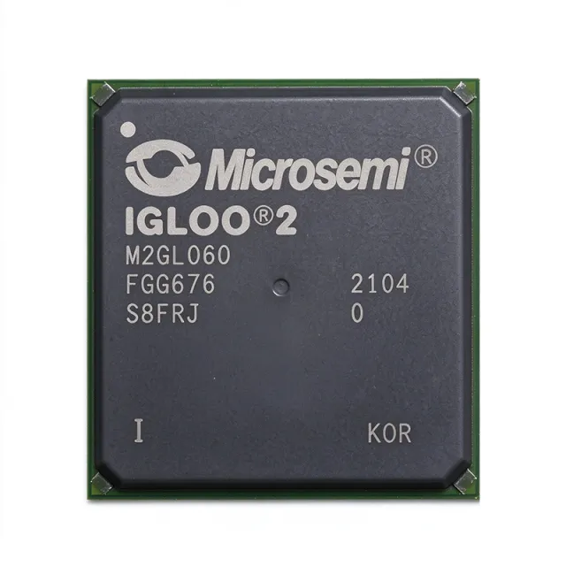
M2GL090-1FGG484
M2GL090-1FGG484 - 86K LEs, 267 I/O, 1.2V IGLOO2 FPGA
The Microchip Technology M2GL090-1FGG484 is an IGLOO2 low-density FPGA with 86,316 logic elements, 267 user I/O, and a 1.2 V operating supply in a 484-ball FBGA package. It provides programmable logic resources for bridging, I/O expansion and conversion, system management, secure connectivity, communications, industrial control, and embedded video or image processing. The -1 suffix denotes the manufacturer's speed grade, while FGG484 identifies the 484-ball package configuration.
An FPGA is a reconfigurable digital semiconductor whose internal look-up tables, flip-flops, routing resources, memory blocks, and programmable I/O can be configured after manufacture. The M2GL090 belongs to the IGLOO2 hierarchy: low-density FPGA, programmable logic device, integrated circuit, and semiconductor. This positioning makes it suitable for consolidating control logic, protocol conversion, and interface adaptation that would otherwise require multiple discrete programmable or glue-logic devices.
The principal device figures are 86,316 logic elements, 267 user I/O, and a 1.2 V supply voltage. Its broad I/O count is valuable for systems requiring numerous digital connections, while the logic capacity supports parallel control, data acquisition, packet handling, and interface bridging. Unlike a fixed-function microcontroller, the FPGA can adapt its internal architecture and pin behavior when the system design changes, reducing external logic and shortening development cycles.
Microchip positions IGLOO2 devices for general-purpose functions including Gigabit Ethernet or dual PCI Express control planes, bridging, input/output expansion and conversion, video and image processing, system management, and secure connectivity. The M2GL090 family is therefore appropriate when deterministic parallel logic, flexible I/O, and post-configuration modification are more important than the simplicity of a software-only control path.
Typical applications include industrial protocol converters, camera and imaging interfaces, secure network-edge equipment, automated test systems, embedded control panels, and communications infrastructure. The 267-I/O device can consolidate high-pin-count interfaces, although each design still requires bank-specific voltage planning, power sequencing, and careful PCB escape routing around the FBGA array.
A key design consideration is migration from smaller IGLOO2 devices. The same 484-ball package can be used across M2GL025, M2GL050, and M2GL090 families, but global-pin availability differs, so unused globals must be checked explicitly in the package pin-description guide. Power, interface standards, and FPGA timing constraints should also be evaluated before reusing a board across density grades.
This page combines manufacturer and distributor lifecycle information, package and logic specifications, drop-in family alternatives, application guidance, and migration-oriented design notes. It is intended to help engineers identify the correct IGLOO2 density, package, and speed-grade combination without overlooking differences in temperature rating, suffix coding, or device configuration.
詢價
聯絡我們