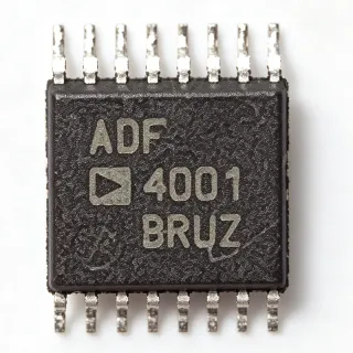
AD5316ARU - Quad 10-Bit DAC, 2.5-5.5V | Analog Devices
MPN: AD5316ARU ✓ 啟用中AD5316ARU 概覽
A digital-to-analog converter is an interface IC that converts digital control words into proportional analog voltages. The AD5316 belongs to the DAC hierarchy, where it sits between a digital bus and precision analog test, control, or instrumentation circuitry. Its buffered outputs reduce the need for external output amplifiers when driving moderate loads.
The four converters provide 10-bit resolution, and the A-grade device has an integral nonlinearity specification of ±4 LSB. On-chip output amplifiers support rail-to-rail output swing with a slew rate of 0.7 V/µs. The single-supply operating range covers both 3.3 V and 5 V systems, while the typical supply current is 500 µA at 3 V for low-power portable and industrial designs.
The AD5316 uses a 2-wire serial interface operating up to 400 kHz and is compatible with SMBus-style communication. Each channel provides an independently programmable output voltage through its corresponding DAC register. The interface allows a microcontroller, embedded processor, or programmable controller to update four analog outputs while minimizing the number of signal connections required on the PCB.
Typical applications include process-control setpoints, automated test equipment, sensor excitation and bias control, industrial data acquisition, programmable laboratory supplies, and low-power embedded instrumentation. The quad-channel arrangement is particularly useful when a system requires several independently controlled analog outputs but has limited connector and routing space.
PCB design should keep the serial interface and output routing compact while observing the analog-ground and supply-return paths recommended in the manufacturer datasheet. Decoupling capacitance should be placed close to the supply pins, and output loads should be checked against the buffered-output capabilities. The 0.7 V/µs slew rate should also be considered when designing waveforms that require rapid output transitions.
This page combines the manufacturer's device characteristics, package and interface details, comparison guidance, and practical application guidance to help engineers evaluate the AD5316ARU without relying only on a basic catalog listing.
直接替換替代品,適用於 AD5316ARU — 相同封裝,腳位對腳位相容。需重新設計 PCB 的不同封裝零件不列入。
AD5316ARUZ
✅ 直接替換📋 參考替代品(不在目錄中)
AD5316ARU-REEL7
✅ 直接替換📋 參考替代品(不在目錄中)
AD5306ARUZ
✅ 直接替換📋 參考替代品(不在目錄中)
AD5317BRUZ
✅ 直接替換📋 參考替代品(不在目錄中)
AD5316RBRUZ
✅ 直接替換📋 參考替代品(不在目錄中)
AD5316ARU 最大額定值與電氣特性
| Number of DAC Channels | 4 channels |
| DAC Resolution | 10 bits |
| Supply Voltage Range | 2.5 V to 5.5 V |
| Typical Supply Current | 500 µA at 3 V |
| 輸出類型 | Buffered voltage output |
| Output Swing | Rail-to-rail |
| Output Slew Rate | 0.7 V/µs |
| Integral Nonlinearity | ±4 LSB for A grade |
| Serial Interface | 2-wire serial interface |
| Maximum Serial Clock Rate | 400 kHz |
| Serial Interface Compatibility | SMBus-compatible |
| Reference Type | External reference |
| 封裝 | 16-lead TSSOP |
| 腳位數 | 16 pins |
| 安裝類型 | Surface mount |
| 工作溫度範圍 | -40 °C to +105 °C |
| Screening Level | Industrial |
| Power Dissipation | 2.5 mW |
| RoHS 狀態 | unknown |
| REACH Status | unknown |
AD5316ARU 16-lead tssop 腳位配置指南
AD5316ARU(16-lead tssop 封裝)的腳位配置。 此類比元件具有輸入、輸出與電源腳位。偏移歸零、補償與致能腳位配置請參閱製造商資料表。適用於訊號調理與放大器電路。

無詳細腳位定義資料: AD5316ARU.
請參閱 資料表 以查看完整腳位配置。
典型應用
AD5316ARU 適用於 6 應用s: Industrial Process Control, Programmable Test Equipment, Sensor Excitation and Biasing, Programmable Laboratory Supplies, Data Acquisition Systems, Embedded Instrumentation.
Industrial Process Control
The AD5316ARU fits four-channel process-control systems that must convert digital setpoints into analog actuator commands. Its 10-bit resolution provides 1,024 codes per channel, while the four buffered outputs allow multiple control loops to share one controller. The 2-wire interface operates up to 400 kHz, reducing wiring in distributed control equipment, and the 2.5 V to 5.5 V supply range supports both 3.3 V and 5 V industrial controller platforms. Verify the external reference, output range, and load impedance against each loop before production deployment.
推薦
Programmable Test Equipment
The AD5316ARU can generate up to four independent analog test stimuli in programmable instrumentation. A 10-bit command word gives each channel 1,024 output levels, which is useful for coarse source calibration, relay or amplifier control, and fixture biasing. Its 400 kHz 2-wire interface allows a test controller to load a sequence of channel values efficiently, while buffered outputs reduce the need for separate output amplifiers. For metrology paths demanding finer resolution, use a higher-resolution DAC and recalibrate the source path.
推薦
Sensor Excitation and Biasing
The AD5316ARU is suitable for multi-channel sensor-bias and excitation systems where four independently adjustable voltages are needed. By placing each DAC output near the associated input network, the 2-wire architecture reduces routing across a measurement board. The 0.7 V/µs output slew rate supports relatively quick settling after code changes, and the low 500 µA typical supply current at 3 V suits compact acquisition modules. Confirm output settling at the required accuracy and ensure the external reference does not introduce noise into the measurement front end.
推薦
Programmable Laboratory Supplies
A laboratory supply controller can use the AD5316ARU to generate four low-level voltage commands for DUT bias, limit setting, or calibration fixtures. The device's 10-bit resolution and rail-to-rail buffered outputs are appropriate when the control path does not require ultra-high precision. Since the outputs are voltage commands rather than direct power-stage drivers, the design should add appropriate amplifiers when driving heavier loads. The 400 kHz serial rate permits coordinated multi-channel updates, which is useful for matching polarity or level changes across a fixture.
推薦
Data Acquisition Systems
The AD5316ARU can supply programmable control or excitation voltages in compact data-acquisition equipment. Four channels let the acquisition controller manage several analog output functions without allocating a separate DAC package for each signal. The 2.5 V minimum supply supports low-voltage embedded designs, while the typical 500 µA current at 3 V helps limit power demand. The serial interface should be routed away from high-gain analog inputs, and the reference and DAC return paths should be arranged according to the manufacturer's layout guidance.
推薦
Embedded Instrumentation
The AD5316ARU is appropriate for embedded instrumentation that needs multiple analog control outputs without adding extensive digital wiring. Its four 10-bit channels and SMBus-compatible 2-wire interface align with microcontroller-based instrumentation, while the TSSOP-16 package supports compact board layouts. The buffered outputs can drive normal instrumentation signal-conditioning inputs, but external buffering may be required for high capacitance or long cable runs. Account for the 0.7 V/µs slew rate when sequencing commands through switched test paths.
推薦
推薦產品摘要
工程參考資料,適用於 AD5316ARU — 比較、設計指引及合規資訊。
選型指南
與替代品比較
| 參數 | 本產品 | AD5316ARUZ | AD5316ARU-REEL7 | AD5306ARUZ | AD5317BRUZ | AD5316RBRUZ |
|---|---|---|---|---|---|---|
| Package | TSSOP-16 | TSSOP-16 | TSSOP-16 | TSSOP-16 | TSSOP-16 | TSSOP-16 |
| Brand | Analog Devices | Analog Devices | Analog Devices | Analog Devices | Analog Devices | Analog Devices |
| Number of DAC Channels | 4 channels | 4 channels | 4 channels | 4 channels | 4 channels | 4 channels |
主要差異化特點
- Exact AD5316ARU ordering configuration (對比AD5316ARUZ)
- Balanced resolution for multichannel control (對比AD5306ARUZ)
- External-reference architecture (對比AD5316RBRUZ)
設計說明
Place the supply bypass capacitor directly between the supply and ground pins, and keep the external reference and reference-return traces short. Route the 2-wire interface away from the four analog outputs and sensitive input circuits. The TSSOP-16 footprint is compact, so leaving adequate spacing around the pins improves soldering access and reduces the chance of accidental bridges between adjacent nets.
Use the manufacturer pin-description table when assigning the SDA-like clock, SCL-like data, reference, supply, ground, and four analog-output nets. Verify that each output trace has a return path and is not routed beside a switching node. If an output drives a capacitive load, keep the load modest or add an isolation resistor and external buffer because the 0.7 V/µs slew rate can produce edge-related settling and crosstalk.
Do not treat a family member with the same package as automatically interchangeable. Confirm pin numbering, accuracy grade, temperature rating, reference voltage, output range, interface protocol, and ordering suffix before replacing the AD5316ARU. The AD5316R family adds an internal reference and power-on-reset functionality, so its control behavior may differ even though all listed alternatives use a TSSOP-16 package.
合規資訊
The device is described as an industrial-grade component, but no specific RoHS, REACH, halogen-free, lead-free, or conflict-minerals declaration is stated on the manufacturer product page. The AD5316ARU is not presented as an AEC-Q100-qualified automotive device.