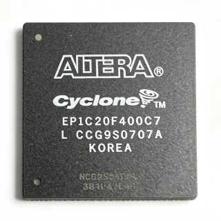
EP1C4F400C6 - Cyclone FPGA, 4000 Cells, 400-BGA | Intel
MPN: EP1C4F400C6 ⚠ 最後購買機會EP1C4F400C6 概覽
A Field Programmable Gate Array (FPGA) is a semiconductor device built around an array of configurable logic blocks (CLBs/LEs) connected by programmable interconnect, allowing hardware engineers to implement arbitrary digital logic that is re-programmable in-circuit. Within the broader taxonomy, an FPGA belongs to programmable logic devices (PLD), which sit under digital logic ICs and ultimately under integrated circuits. The Cyclone family sits at the entry-level / low-cost tier of the FPGA hierarchy, above simple CPLDs but below the Stratix high-performance tier.
Key features of the EP1C4F400C6 include 4,000 logic elements distributed across 400 LABs, 301 user I/O pins (supporting LVTTL, LVCMOS, SSTL, and LVDS), 78 Kbits of M4K embedded RAM blocks, two PLLs for clock management, and support for external memory interfaces including SDR SDRAM, FCRAM, and SRAM. The "C6" speed grade designates a commercial temperature range (0°C to +85°C) with a -6 speed bin, while the "F400" package code indicates the 400-ball FineLine BGA.
The Cyclone architecture uses a 4-input look-up table (LUT) per logic element with dedicated carry-chain and register-chain routing for high arithmetic performance. The 130nm process and 1.5V core supply keep dynamic power manageable for high-volume consumer, industrial, and communications designs, while the embedded M4K blocks enable efficient on-chip FIFOs, buffering, and small memory-mapped data paths.
Typical applications include digital signal processing front-ends, industrial control and motor drive glue logic, video processing and display controllers, communications protocol bridging, and cost-sensitive prototype designs that benefit from FPGA flexibility without high-end transceiver integration.
When designing with this device, careful attention must be paid to power distribution across the 400-ball BGA, signal-integrity-driven PCB stackup, and I/O bank VCCIO planning, since mixed-voltage I/O standards require per-bank supply rails.
This page synthesizes distributor pricing, same-family drop-in alternatives, and practical design notes not collected in any single manufacturer document.
直接替換替代品,適用於 EP1C4F400C6 — 相同封裝,腳位對腳位相容。需重新設計 PCB 的不同封裝零件不列入。
此系列的變體
與下列產品可直接替換的同系列型號: EP1C4F400C6 (相同外形與佔位) — 差異在於 Speed Grade, Package, Family, Operating Temperature, Total RAM Bits.
EP1C4F400C8N
✅ 直接替換聯絡詢價
查看資料表 →EP1C4F400C7N
✅ 直接替換聯絡詢價
查看資料表 →EP1C4F400I7N
✅ 直接替換聯絡詢價
查看資料表 →EP1C4F400C6N
✅ 直接替換聯絡詢價
查看資料表 →EP1C4F400C7
✅ 直接替換聯絡詢價
查看資料表 →EP1C4F400C6 最大額定值與電氣特性
| Family | Cyclone |
| Logic Elements | 4,000 |
| Logic Array Blocks (LABs) | 400 |
| Total RAM Bits | 78,000 |
| Embedded RAM Blocks | M4K |
| User I/O Pins | 301 |
| PLLs | 2 |
| 封裝 | 400-ball FineLine BGA (FBGA-400) |
| Process Technology | 130 nm CMOS |
| Core Voltage | 1.5 V |
| Speed Grade | -6 (commercial) |
| 工作溫度 | 0°C to +85°C (commercial) |
| 安裝類型 | Surface Mount (BGA) |
EP1C4F400C6 400-ball fineline bga (fbga-400) 腳位配置指南
EP1C4F400C6(400-ball fineline bga (fbga-400) 封裝)的腳位配置。 此數位 IC 包含 GPIO、通訊介面(UART、SPI、I2C)與電源腳位。替代腳位功能與配置選項請參閱製造商資料表。對嵌入式系統設計與 PCB 佈局至關重要。

無詳細腳位定義資料: EP1C4F400C6.
請參閱 資料表 以查看完整腳位配置。
典型應用
EP1C4F400C6 適用於 6 應用s: Industrial Control and Glue Logic, Digital Signal Processing Front-End, Video Processing and Display Controllers, Communications Protocol Bridging, Cost-Sensitive Prototype and Evaluation Designs, Legacy Equipment Modernization and Long-Life Programs.
Industrial Control and Glue Logic
The EP1C4F400C6 is well suited to industrial control and motor-drive glue logic where 4,000 logic elements, 301 user I/Os, and two PLLs provide more than enough capacity for state machines, encoder interfaces, and PWM generation. Its commercial temperature range (0°C to +85°C) covers most factory-floor enclosures with active cooling. The 400-ball BGA enables dense board layouts, while the M4K RAM blocks implement command FIFOs and look-up tables for sensor linearization.
推薦
Digital Signal Processing Front-End
For low-cost DSP front-ends such as audio sample-rate conversion, FIR/IIR filter banks, or simple FFT pre-processing, the EP1C4F400C6's 4,000 LEs and 78 Kbits of embedded RAM provide adequate resources for moderate-complexity algorithms at audio and baseband sample rates. The two PLLs generate the precise clock trees required for ADC/DAC synchronization, and the LVDS-capable I/Os interface directly to common audio and video ADCs without external translators.
推薦
Video Processing and Display Controllers
The EP1C4F400C6 is commonly deployed in video format conversion, de-interlacing, and LCD/TFT timing generator designs. Its 301 user I/Os comfortably drive 24-bit RGB plus control and sync signals, while the M4K RAM blocks implement line buffers and color lookup tables. Designers use the LVDS I/O capability to interface directly to LVDS panel inputs, eliminating external serializer components and reducing BOM cost in consumer displays.
推薦
Communications Protocol Bridging
Bridge designs converting between UART, SPI, I2C, parallel buses, and legacy telecom interfaces fit naturally in 4,000 LEs. The EP1C4F400C6's abundant user I/Os (301) make it ideal for multi-channel protocol aggregation, while the M4K blocks buffer packet payloads between asynchronous clock domains. Industrial protocol stacks such as Modbus, Profibus, and CAN glue logic are easily implemented, making this part a common choice for legacy equipment modernization.
推薦
Cost-Sensitive Prototype and Evaluation Designs
Designers building FPGA-based prototypes for ASIC validation, university teaching platforms, or low-volume OEM products appreciate the EP1C4F400C6's balance of capacity and price. Quartus II Web Edition (free) supports the full Cyclone family, eliminating software licensing friction. The 400-ball BGA exposes enough I/Os for daughter-card expansion, and the abundant M4K RAM enables realistic test benches with realistic data buffering requirements.
推薦
Legacy Equipment Modernization and Long-Life Programs
Many defense, aerospace, and medical OEMs have Cyclone I designs that must continue manufacturing for 10-20 year life cycles. Because the EP1C4F400C6 is on Intel's last-time-buy list (as of 2026-09-06), these programs are stockpiling inventory and qualifying drop-in alternatives such as the EP1C4F400C8N and EP1C4F400I7N. These parts share the same die, package, and pinout, allowing form-fit-function continuity without PCB redesign.
推薦
推薦產品摘要
工程參考資料,適用於 EP1C4F400C6 — 比較、設計指引及合規資訊。
選型指南
與替代品比較
| 參數 | 本產品 | EP1C4F400C8N | EP1C4F400C7N | EP1C4F400I7N | EP1C4F400C6N | EP1C4F400C7 |
|---|---|---|---|---|---|---|
| Brand | Intel | Intel | Intel | Intel | Intel | Intel |
| Package | 400-ball FineLine BGA | 400-ball FineLine BGA (same) | 400-ball FineLine BGA (same) | 400-ball FineLine BGA (same) | 400-ball FineLine BGA (same) | 400-ball FineLine BGA (same) |
| Logic Elements | 4,000 | 4,000 | 4,000 | 4,000 | 4,000 | 4,000 |
| LABs | 400 | 400 | 400 | 400 | 400 | 400 |
| User I/Os | 301 | 301 | 301 | 301 | 301 | 301 |
| Speed Grade | -6 | -8 | -7 | -7 | -6 | -7 |
| Temperature Range | 0°C to +85°C (commercial) | 0°C to +85°C (commercial) | 0°C to +85°C (commercial) | -40°C to +100°C (industrial) | 0°C to +85°C (commercial) | 0°C to +85°C (commercial) |
| Lead-Free Finish | No (leaded, C6 suffix) | Yes (N suffix) | Yes (N suffix) | Yes (N suffix) | Yes (N suffix) | No (leaded) |
| Lifecycle Status | Last-Time-Buy | Last-Time-Buy | Last-Time-Buy | Last-Time-Buy | Last-Time-Buy | Last-Time-Buy |
主要差異化特點
- Lowest-cost 4,000-LE Cyclone variant with -6 speed grade (對比EP1C4F400C8N)
- Commercial temperature range matches cost-driven designs (對比EP1C4F400I7N)
- Leaded terminal finish for legacy manufacturing compatibility (對比EP1C4F400C6N)
設計說明
The 400-ball FineLine BGA uses a 1.0 mm ball pitch, which mandates a 4-layer or 6-layer PCB stackup with microvia or sub-merged via technology for fan-out. Route all VCCINT (1.5V core) and VCCIO (per-bank I/O supply) rails with wide power planes and place 0.1 µF + 10 µF decoupling capacitors within 100 mil of every supply pin. Use a continuous GND plane on the layer immediately beneath the BGA to provide a low-impedance return path and to dissipate the 1.5W to 3W typical device power.
Estimated: at 100% logic utilization with 200 MHz internal clock, the EP1C4F400C6 dissipates approximately 1.5 W to 3 W. With a typical junction-to-ambient thermal resistance (θJA) of 12 °C/W for a 400-ball BGA on a 4-layer JEDEC test board, junction temperature rise above ambient is ~36 °C. For sustained high-activity designs, ensure at least 8 thermal vias in the BGA center pad to the internal GND plane to maintain junction temperature below 125 °C.
Do not mix LVTTL 3.3V and LVDS 2.5V signals in the same I/O bank without proper VCCIO planning — each bank shares a single VCCIO rail. Floating configuration pins (nCONFIG, nSTATUS, CONF_DONE) can cause undefined startup behavior; tie them through 10 kΩ pull-ups to VCCIO. For JTAG chains, ensure the JTAG pins are not repurposed as general I/O in the Quartus pin planner, or boundary-scan will fail. Finally, do not assume the original Cyclone bitstream format is compatible with Quartus Prime — use Quartus II 13.0sp1 or earlier for compilation.
合規資訊
EP1C4F400C6 has a leaded (SnPb) terminal finish per the 'no N-suffix' convention; RoHS/REACH status not explicitly stated in verified data. Industrial variants (I7N suffix) and lead-free variants (N suffix) exist for compliant builds.