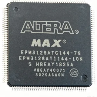
EPM3256ATI144-7N - 256-Macrocell MAX 3000A CPLD, 7.5ns, TQFP-144 | Altera
MPN: EPM3256ATI144-7N ✗ 停產EPM3256ATI144-7N 概覽
A CPLD (Complex Programmable Logic Device) is a non-volatile, flash- or EPROM-based programmable logic device that combines multiple PLA-like macrocell blocks on a single chip, sitting between small discrete logic (gates, 74-series ICs) and large FPGAs. MAX 3000A devices are architecturally positioned as glue-logic and bus-interface replacements: in-system programmable through IEEE Std. 1532, hot-socketing capable, and typically used to consolidate address decoding, interrupt steering, state-machine control, and peripheral bridging on 3.3 V/5 V boards. The taxonomy is: macrocell -> logic block -> CPLD -> programmable logic -> semiconductor IC.
Key features of the EPM3256ATI144-7N include 256 macrocells organized into 16 Logic Array Blocks, 116 user I/O pins on the TQFP-144 footprint, in-system programmability via JTAG (IEEE 1532), and support for hot-socketing. The MultiVolt I/O interface lets the core run at 3.3 V while output banks independently drive 5.0 V, 3.3 V, or 2.5 V loads. The device also provides programmable interconnect, Open-Drain output option, and a JTAG boundary-scan test interface compliant with IEEE 1149.1.
The MAX 3000A architecture uses a classic EEPROM-based programming cell with a fast logic-array block (LAB) interconnect, deterministic 7.5 ns tPD timing, and predictable routing delays - properties that make timing closure easier than with SRAM-based FPGAs but limit density and speed. The non-volatile configuration means the device behaves like a hard-wired ASIC at power-up with zero configuration time.
Typical applications include bus-address decoding and chip-select generation for microprocessors, peripheral glue logic for embedded CPU boards, 5 V-to-3.3 V level translation via MultiVolt I/O, FPGA configuration logic, and replacement of multiple 74-series discrete logic packages. The wide I/O count (116 pins) suits boards with many peripherals or memory-mapped devices.
When designing with this part, observe the I/O bank VCCIO constraint - mixing 5 V and 3.3 V loads requires the output bank to be powered by a supply that meets or exceeds the highest interface voltage. Decouple every VCCINT and VCCIO pin with 0.1 microfarat ceramic capacitors placed close to the package.
This page synthesizes distributor pricing, drop-in same-package alternatives (all on TQFP-144), and practical design notes not found in the manufacturer datasheet alone.
直接替換替代品,適用於 EPM3256ATI144-7N — 相同封裝,腳位對腳位相容。需重新設計 PCB 的不同封裝零件不列入。
此系列的變體
與下列產品可直接替換的同系列型號: EPM3256ATI144-7N (相同外形與佔位) — 差異在於 Package, Operating Temperature, Propagation Delay (tPD), RoHS Status, JTAG Support.
EPM3256ATC144-7N
✅ 直接替換聯絡詢價
查看資料表 →EPM3256ATI144-10N
✅ 直接替換聯絡詢價
查看資料表 →EPM3256ATC144-10N
✅ 直接替換聯絡詢價
查看資料表 →EPM3256ATC144-7
✅ 直接替換 ⚠️ 規格未經驗證聯絡詢價
查看資料表 →EPM3256ATC144-10
✅ 直接替換 ⚠️ 規格未經驗證聯絡詢價
查看資料表 →EPM3256ATI144-10
✅ 直接替換 ⚠️ 規格未經驗證聯絡詢價
查看資料表 →EPM3256ATI144-7N 最大額定值與電氣特性
| Family | MAX 3000A |
| Device Type | CPLD (Complex Programmable Logic Device) |
| Macrocells | 256 |
| Usable Gates | 5,000 |
| Logic Array Blocks (LABs) | 16 |
| Maximum User I/O Pins | 116 |
| Propagation Delay (tPD) | 7.5 ns (typical) |
| Maximum Internal Frequency | 126.6 MHz |
| Core Supply Voltage (VCCINT) | 3.3 V |
| I/O Supply Voltage (VCCIO) | 3.3 V or 2.5 V |
| MultiVolt I/O Logic Levels | 5.0 V / 3.3 V / 2.5 V |
| Programming Technology | EEPROM (in-system programmable) |
| JTAG / ISP | IEEE Std. 1532 compliant |
| Boundary Scan | IEEE Std. 1149.1 (JTAG) |
| Hot-Socketing Support | Yes |
| 封裝 | TQFP-144 (20 x 20 mm, 0.5 mm pitch) |
| 工作溫度 | -40C to +85C (industrial) |
| RoHS 狀態 | Compliant (lead-free) |
EPM3256ATI144-7N 腳位配置
| 腳位 1 | I/O — User I/O pin |
| 腳位 2 | I/O — User I/O pin |
| 腳位 3 | I/O — User I/O pin |
| 腳位 4 | I/O — User I/O pin |
| 腳位 5 | I/O — User I/O pin |
| 腳位 6 | I/O — User I/O pin |
| 腳位 7 | I/O — User I/O pin |
| 腳位 8 | VCCINT — Core supply (3.3 V) |
| 腳位 9 | I/O — User I/O pin |
| 腳位 10 | I/O — User I/O pin |
| 腳位 11 | GND — Ground |
| 腳位 12 | I/O — User I/O pin |
| 腳位 13 | I/O — User I/O pin |
| 腳位 14 | I/O — User I/O pin |
| 腳位 15 | I/O — User I/O pin |
| 腳位 16 | I/O — User I/O pin |
| 腳位 17 | I/O — User I/O pin |
| 腳位 18 | I/O — User I/O pin |
| 腳位 19 | I/O — User I/O pin |
| 腳位 20 | I/O — User I/O pin |
| 腳位 21 | I/O — User I/O pin |
| 腳位 22 | I/O — User I/O pin |
| 腳位 23 | GND — Ground |
| 腳位 24 | I/O — User I/O pin |
| 腳位 25 | I/O — User I/O pin |
| 腳位 26 | I/O — User I/O pin |
| 腳位 27 | I/O — User I/O pin |
| 腳位 28 | I/O — User I/O pin |
| 腳位 29 | I/O — User I/O pin |
| 腳位 30 | I/O — User I/O pin |
| 腳位 31 | I/O — User I/O pin |
| 腳位 32 | I/O — User I/O pin |
| 腳位 33 | I/O — User I/O pin |
| 腳位 34 | VCCINT — Core supply (3.3 V) |
| 腳位 35 | I/O — User I/O pin |
| 腳位 36 | I/O — User I/O pin |
| 腳位 37 | GND — Ground |
| 腳位 38 | I/O — User I/O pin |
| 腳位 39 | I/O — User I/O pin |
| 腳位 40 | I/O — User I/O pin |
| 腳位 41 | I/O — User I/O pin |
| 腳位 42 | I/O — User I/O pin |
| 腳位 43 | I/O — User I/O pin |
| 腳位 44 | I/O — User I/O pin |
| 腳位 45 | I/O — User I/O pin |
| 腳位 46 | I/O — User I/O pin |
| 腳位 47 | I/O — User I/O pin |
| 腳位 48 | I/O — User I/O pin |
| 腳位 49 | GND — Ground |
| 腳位 50 | I/O — User I/O pin |
| 腳位 51 | I/O — User I/O pin |
| 腳位 52 | I/O — User I/O pin |
| 腳位 53 | I/O — User I/O pin |
| 腳位 54 | I/O — User I/O pin |
| 腳位 55 | I/O — User I/O pin |
| 腳位 56 | I/O — User I/O pin |
| 腳位 57 | I/O — User I/O pin |
| 腳位 58 | I/O — User I/O pin |
| 腳位 59 | VCCINT — Core supply (3.3 V) |
| 腳位 60 | I/O — User I/O pin |
| 腳位 61 | I/O — User I/O pin |
| 腳位 62 | GND — Ground |
| 腳位 63 | I/O — User I/O pin |
| 腳位 64 | I/O — User I/O pin |
| 腳位 65 | I/O — User I/O pin |
| 腳位 66 | I/O — User I/O pin |
| 腳位 67 | I/O — User I/O pin |
| 腳位 68 | I/O — User I/O pin |
| 腳位 69 | I/O — User I/O pin |
| 腳位 70 | I/O — User I/O pin |
| 腳位 71 | I/O — User I/O pin |
| 腳位 72 | I/O — User I/O pin |
| 腳位 73 | GND — Ground |
| 腳位 74 | I/O — User I/O pin |
| 腳位 75 | I/O — User I/O pin |
| 腳位 76 | I/O — User I/O pin |
| 腳位 77 | I/O — User I/O pin |
| 腳位 78 | I/O — User I/O pin |
| 腳位 79 | I/O — User I/O pin |
| 腳位 80 | I/O — User I/O pin |
| 腳位 81 | I/O — User I/O pin |
| 腳位 82 | I/O — User I/O pin |
| 腳位 83 | I/O — User I/O pin |
| 腳位 84 | VCCINT — Core supply (3.3 V) |
| 腳位 85 | I/O — User I/O pin |
| 腳位 86 | I/O — User I/O pin |
| 腳位 87 | GND — Ground |
| 腳位 88 | I/O — User I/O pin |
| 腳位 89 | I/O — User I/O pin |
| 腳位 90 | I/O — User I/O pin |
| 腳位 91 | I/O — User I/O pin |
| 腳位 92 | I/O — User I/O pin |
| 腳位 93 | I/O — User I/O pin |
| 腳位 94 | I/O — User I/O pin |
| 腳位 95 | I/O — User I/O pin |
| 腳位 96 | I/O — User I/O pin |
| 腳位 97 | GND — Ground |
| 腳位 98 | I/O — User I/O pin |
| 腳位 99 | I/O — User I/O pin |
| 腳位 100 | I/O — User I/O pin |
| 腳位 101 | I/O — User I/O pin |
| 腳位 102 | I/O — User I/O pin |
| 腳位 103 | I/O — User I/O pin |
| 腳位 104 | I/O — User I/O pin |
| 腳位 105 | I/O — User I/O pin |
| 腳位 106 | I/O — User I/O pin |
| 腳位 107 | I/O — User I/O pin |
| 腳位 108 | I/O — User I/O pin |
| 腳位 109 | VCCINT — Core supply (3.3 V) |
| 腳位 110 | TDI — JTAG Test Data In |
| 腳位 111 | TMS — JTAG Test Mode Select |
| 腳位 112 | TCK — JTAG Test Clock |
| 腳位 113 | GND — Ground |
| 腳位 114 | TDO — JTAG Test Data Out |
| 腳位 115 | I/O — User I/O pin |
| 腳位 116 | I/O — User I/O pin |
| 腳位 117 | I/O — User I/O pin |
| 腳位 118 | I/O — User I/O pin |
| 腳位 119 | I/O — User I/O pin |
| 腳位 120 | I/O — User I/O pin |
| 腳位 121 | GND — Ground |
| 腳位 122 | I/O — User I/O pin |
| 腳位 123 | I/O — User I/O pin |
| 腳位 124 | I/O — User I/O pin |
| 腳位 125 | I/O — User I/O pin |
| 腳位 126 | I/O — User I/O pin |
| 腳位 127 | I/O — User I/O pin |
| 腳位 128 | I/O — User I/O pin |
| 腳位 129 | I/O — User I/O pin |
| 腳位 130 | I/O — User I/O pin |
| 腳位 131 | I/O — User I/O pin |
| 腳位 132 | VCCINT — Core supply (3.3 V) |
| 腳位 133 | GCLK1 — Global clock input 1 |
| 腳位 134 | OE1 — Global output enable 1 |
| 腳位 135 | CLR — Global clear |
| 腳位 136 | I/O — User I/O pin |
| 腳位 137 | I/O — User I/O pin |
| 腳位 138 | GND — Ground |
| 腳位 139 | I/O — User I/O pin |
| 腳位 140 | I/O — User I/O pin |
| 腳位 141 | GCLK2 — Global clock input 2 |
| 腳位 142 | OE2 — Global output enable 2 |
| 腳位 143 | INPUT — Dedicated input |
| 腳位 144 | I/O — User I/O pin |
典型應用
EPM3256ATI144-7N 適用於 6 應用s: Microprocessor Bus Address Decoding, FPGA Configuration Logic and Glue Logic, Mixed-Voltage 5V to 3.3V Level Translation Interface, Peripheral Glue Logic for Embedded CPU Boards, Legacy Industrial Control and Test Equipment, State Machine Control and Sequencing Logic.
Microprocessor Bus Address Decoding
The EPM3256ATI144-7N is well suited to generate chip-select signals for microprocessor address buses. With 256 macrocells and 7.5 ns tPD, it can decode a 24-bit address space with multiple memory and peripheral windows, replacing 8 to 15 discrete 74LS138/139/688 decoder and comparator packages. The 3.3 V core plus MultiVolt I/O allows direct interface to 5 V-tolerant memory buses (e.g., legacy 8051, ISA-bus designs) without level shifters. The device is in-system programmable via JTAG, so address maps can be revised late in the design cycle, accelerating prototype bring-up.
推薦
FPGA Configuration Logic and Glue Logic
In FPGA-based designs, the EPM3256ATI144-7N serves as a configuration controller and glue-logic partner: it handles multi-FPGA configuration sequencing, generates configuration clocks, monitors DONE/MODE pins, and bridges between the host CPU bus and the FPGA control/status registers. The non-volatile EEPROM-based MAX 3000A configuration means the device is ready in microseconds at power-up, with no external configuration memory. Its 116 user I/Os comfortably support multi-FPGA boards and peripheral expansion, while MultiVolt I/O bridges 5 V legacy peripherals to 3.3 V FPGA I/O banks.
推薦
Mixed-Voltage 5V to 3.3V Level Translation Interface
The MultiVolt I/O architecture makes the EPM3256ATI144-7N an effective level-translation bridge between 5 V legacy peripherals and 3.3 V modern logic. By connecting the VCCIO bank supply to 5 V, the I/O pins can directly drive or receive 5 V TTL levels, while the 3.3 V core talks to 3.3 V peripherals on a different bank. This eliminates discrete level-shifter ICs (TXB0108, SN74LVC4245) and reduces BOM count in mixed-voltage legacy-modern interface designs such as industrial controllers, test instruments, and PCI-to-PCIe adapter boards.
推薦
Peripheral Glue Logic for Embedded CPU Boards
Embedded CPU boards using ARM, MIPS, or x86 processors often require many small logic functions: address latches, chip selects, interrupt steering, reset distribution, watchdog timers, and bus multiplexers. The EPM3256ATI144-7N consolidates these functions into one device with 256 macrocells and 116 I/Os, replacing 15 to 30 discrete 74-series packages. With in-system programmability, the same board design can be re-targeted to different processor variants or bus topologies by re-flashing the CPLD via JTAG, simplifying NPI and shortening time-to-market.
推薦
Legacy Industrial Control and Test Equipment
Industrial PLCs, motor controllers, and bench test instruments from the late 1990s through 2010s frequently use the MAX 3000A family for state-machine control, sequencing, and timing-critical I/O handling. The EPM3256ATI144-7N, with its industrial -40C to +85C temperature range and RoHS-compliant TQFP-144 package, is well suited for these long-lifecycle applications where redesign is impractical. The deterministic 7.5 ns tPD simplifies worst-case timing analysis, which is valuable in safety-critical control loops where every nanosecond of jitter matters.
推薦
State Machine Control and Sequencing Logic
Complex finite-state machines with 16 to 64 states, parallel datapath control, and microsequencer-style instruction decoding are a classic CPLD use case. The EPM3256ATI144-7N's 16 Logic Array Blocks, deterministic 7.5 ns tPD, and rich register resources make it suitable for protocol engines (I2C, SPI, UART, custom buses), disk-drive controllers, and timing-critical industrial protocols. Designers can implement deep state machines with synchronous register outputs, three-state bus drivers, and Open-Drain options for wire-OR signaling on a single chip.
推薦
推薦產品摘要
工程參考資料,適用於 EPM3256ATI144-7N — 比較、設計指引及合規資訊。
選型指南
與替代品比較
| 參數 | 本產品 | EPM3256ATC144-7N | EPM3256ATI144-10N | EPM3256ATC144-10N | EPM3256ATC144-7 |
|---|---|---|---|---|---|
| Package | TQFP-144 | TQFP-144 - same | TQFP-144 - same | TQFP-144 - same | TQFP-144 - same |
| Brand | Altera | Altera | Altera | Altera | Altera |
| Macrocells | 256 | 256 | 256 | 256 | 256 |
| Speed Grade (tPD) | 7 (7.5 ns) | 7 (7.5 ns) - same | 10 (10 ns) - slower | 10 (10 ns) - slower | 7 (7.5 ns) - same |
| Temperature Grade | Industrial (-40C to +85C) | Commercial (0C to +70C) | Industrial (-40C to +85C) - same | Commercial (0C to +70C) | Commercial (0C to +70C) |
| Maximum User I/O | 116 | 116 | 116 | 116 | 116 |
| Maximum Frequency | 126.6 MHz | 126.6 MHz | 100 MHz (slower grade) | 100 MHz (slower grade) | 126.6 MHz |
| Core Voltage (VCCINT) | 3.3 V | 3.3 V | 3.3 V | 3.3 V | 3.3 V |
| Lifecycle Status | Obsolete | Obsolete | Obsolete | Obsolete | Obsolete |
| RoHS Compliance | Compliant (lead-free) | Compliant | Compliant | Compliant | Compliant |
主要差異化特點
- Industrial temperature grade for harsh environments (對比EPM3256ATC144-7N)
- Faster -7 speed grade vs -10 alternatives (對比EPM3256ATI144-10N)
- 116 user I/Os versus smaller MAX 3000A members (對比EPM3128ATC144-10N)
設計說明
Estimated: at typical operating frequency (50 MHz CMOS switching, 50% toggle) the EPM3256ATI144-7N core supply current Iccint is approximately 30 to 60 mA, plus per-bank VCCIO current proportional to the number of switching outputs and load capacitance. Provide a low-impedance 3.3 V rail with at least 200 mA headroom and place a 0.1 microfarad ceramic decoupling capacitor on every VCCINT pin (typically 4 to 6 pins in TQFP-144) plus a bulk 10 microfarad tantalum near the package. VCCIO banks should be decoupled similarly per bank, with the bank supply set to 3.3 V or 2.5 V depending on the logic level of the connected peripherals.
Route all high-speed outputs (clocks, control signals) with controlled-impedance traces (50 ohm typical for CMOS) and keep them short to minimize ringing. Provide a continuous ground plane under the TQFP-144 package and stitch the ground plane with vias around the periphery at 5 to 10 mm spacing to reduce EMI and improve signal integrity. JTAG signals (TCK, TMS, TDI, TDO) should be routed together with a ground guard and terminated at the connector; allow a JTAG header for in-system programming via IEEE Std. 1532.
Do not confuse the VCCINT (3.3 V core) and VCCIO (per-bank I/O supply) pins - mixing them will damage the device. The MultiVolt I/O architecture requires the VCCIO of each bank to be set to the supply voltage of the peripherals it drives, not necessarily 3.3 V. Never leave VCCIO floating - tie every VCCIO pin to either 3.3 V or 2.5 V (or 5 V for legacy 5 V-tolerance, though the -7 industrial grade datasheet specifies 3.3 V/2.5 V for VCCIO). When migrating from the -7 to the -10 speed grade, re-verify timing margins - the 33% slower tPD may break critical paths in designs operating near 100 MHz.
合規資訊
RoHS compliant per Altera/Intel product page (lead-free TQFP-144). Not AEC-Q100 qualified - this is a commercial/industrial CPLD, not an automotive-grade device. Halogen-free status not explicitly stated in the verified web data.