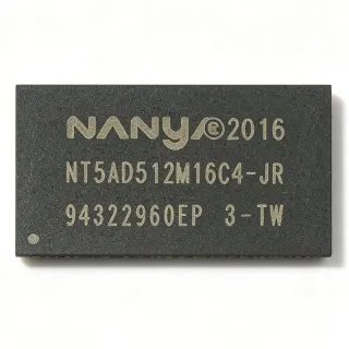
K4A8G165WB-BCTD - 8Gb DDR4 SDRAM 512Mx16 2666Mbps | Samsung
MPN: K4A8G165WB-BCTD ✓ 啟用中K4A8G165WB-BCTD 概覽
DDR4 SDRAM (Double Data Rate Fourth Generation Synchronous Dynamic Random Access Memory) is the JEDEC-standard mainstream DRAM technology used as main memory in PCs, servers, embedded systems, and networking equipment. It succeeds DDR3 with lower operating voltage (1.2V vs 1.5V), higher data rates, bank groups, and improved signaling such as on-die termination and DBI (data bus inversion). Within the memory hierarchy, DDR4 SDRAM sits under synchronous DRAM, random access memory, and semiconductor memory.
Key features of the K4A8G165WB (B-die generation) include 8Gb density in a single die, a 512M x 16 organization that suits systems using 16-bit or 32-bit memory buses without byte-write enable complexity, and a 2666 Mbps/pin data rate (PC4-21300 class, CL19 at 1.2V per JEDEC DDR4 speed bins). The x16 organization provides dedicated data mask (DM) and differential DQS signals per byte lane for reliable high-speed data capture.
Architecturally, the device uses DDR4 bank-group architecture with internal pipelined operations, allowing back-to-back accesses within a bank group at tCCD_S-limited rates and across groups at faster tCCD_L rates. Dynamic on-die termination (ODT), ZQ calibration, and per-byte write leveling support signal integrity across the fly-by routed command/address bus typical of DDR4 designs.
Typical applications include embedded computing boards, industrial PCs, networking switches and routers, set-top boxes, automotive infotainment platforms, and any SoC/FPGA design with a DDR4 x16 memory controller requiring 1GB per chip (8Gb).
Design consideration: maintain the 1.14V-1.26V VDD window and follow the fly-by routing with ODT enabled; validate controller timing at the -TC (2666) bin because speed-bin suffixes are not interchangeable without re-qualification.
This page synthesizes distributor pricing, drop-in alternatives, and practical design notes not found in the manufacturer datasheet.
直接替換替代品,適用於 K4A8G165WB-BCTD — 相同封裝,腳位對腳位相容。需重新設計 PCB 的不同封裝零件不列入。
此系列的變體
與下列產品可直接替換的同系列型號: K4A8G165WB-BCTD (相同外形與佔位) — 差異在於 Data Rate, Operating Temperature, Package, Interface, ZQ Calibration.
K4A8G165WB-BCRC
✅ 直接替換✗ 缺貨
$12.57 / 單位
查看資料表 →K4A8G165WC-BCTD
✅ 直接替換✓ 有庫存
$41.2 / 單位
查看資料表 →K4A8G165WB-BCWE
✅ 直接替換✓ 有庫存
$6.55 / 單位
查看資料表 →MT40A512M16HA-075:E
✅ 直接替換📋 參考替代品(不在目錄中)
H5ANAG8MNJA-UHC
✅ 直接替換📋 參考替代品(不在目錄中)
K4A8G165WB-BCTD 規格
| 記憶體類型 | DDR4 SDRAM |
| Density | 8 Gb |
| 組織 | 512M x 16 |
| 資料速率 | 2666 Mbps |
| Supply Voltage (VDD) | 1.2 V |
| 工作溫度 | 0C to +85C |
| 封裝 | 96FBGA |
| Die Generation | B-die |
| 安裝類型 | Surface Mount (BGA) |
| 介面 | DDR4 (parallel, double data rate) |
| Data Mask | Supported (DM per x16 lane) |
| ZQ Calibration | Supported |
| Dynamic On-Die Termination | Supported |
| RoHS 狀態 | Compliant (per JLCPCB listing: ROHS) |
K4A8G165WB-BCTD 96fbga 腳位配置指南
K4A8G165WB-BCTD(96fbga 封裝)的腳位配置。 腳位編號、功能與連接圖定義於製造商資料手冊中。請參閱該手冊以取得確切的封裝尺寸與焊接指引。

無詳細腳位定義資料: K4A8G165WB-BCTD.
請參閱 資料表 以查看完整腳位配置。
典型應用
K4A8G165WB-BCTD 適用於 6 應用s: Embedded Computing Boards, Networking Switches and Routers, Industrial PCs and HMI Panels, Set-Top Boxes and Smart TV Platforms, Automotive Infotainment (non-safety), Test and Measurement Instruments.
Embedded Computing Boards
Embedded single-board computers and COMs use the K4A8G165WB-BCTD as main memory because its 8Gb density yields 1 GB per chip and its x16 organization matches the 16-bit or 32-bit DDR4 controllers common in ARM SoCs and FPGAs. Placed on a fly-by-routed 2666 Mbps bus with dynamic ODT enabled and ZQ calibration at boot, the device sustains full-bandwidth operation with four-layer stackups when length-matched within +/-25 mils on data lanes. Its commercial 0C to +85C range covers most industrial enclosure conditions, while the 1.2V rail keeps memory power under roughly 0.5 W per chip in typical read/write mixes.
推薦
Networking Switches and Routers
Packet-buffer and control-plane memory in enterprise switches and routers benefits from the K4A8G165WB-BCTD's 2666 Mbps rate and per-lane data mask, which lets firmware perform partial writes into packet descriptors without read-modify-write cycles. Multiple x16 devices are ganged into 32-bit or 64-bit buses for 8-16 GB of buffer memory on the same 96FBGA footprint, and the CRC/CA parity capability improves command-bus integrity in electrically noisy backplane environments. Compared with GDDR or QDR alternatives, DDR4 x16 DRAM offers the best cost per gigabit for buffering at 10G-100G line rates.
推薦
Industrial PCs and HMI Panels
Industrial PCs, machine-vision controllers, and HMI panels deploy the K4A8G165WB-BCTD for frame buffers and application memory. The B-die's stable 2666 Mbps operation at 1.2V gives headroom against supply sag on 24V-derived rails, and the +85C rating covers most fanless enclosures when PCB copper spreads junction heat. The 96FBGA ball array tolerates vibration better than TSOP DDR3 packages, and dynamic on-die termination reduces the number of external termination components, improving reliability in dusty, conductive-contaminant environments typical of factory floors.
推薦
Set-Top Boxes and Smart TV Platforms
Consumer video platforms attach one or two K4A8G165WB-BCTD devices to the SoC's 16/32-bit DDR4 interface to reach 1-2 GB of memory for 4K video decoding at minimum BOM cost. The 2666 Mbps bin matches the bandwidth needed for HEVC multi-stream decode, and the x16 organization eliminates byte-enable complexity on cost-sensitive PCBs. Its 1.2V operation directly satisfies energy-star style standby targets, and the commodity 96FBGA footprint keeps board area small enough for stick-form set-top hardware.
推薦
Automotive Infotainment (non-safety)
Infotainment and cluster SoCs with commercial-range x16 DDR4 controllers use the K4A8G165WB-BCTD in non-safety domains where the 0C to +85C window is acceptable (in-cabin temperature-managed zones). The 8Gb density supports map rendering and multi-display compositing at 2666 Mbps, and CRC on the command/address bus improves robustness against EMI from the vehicle's RF environment. For under-dash installations exceeding +85C, substitute the K4A8G165WC-BCTD with its +95C ceiling; for true AEC-Q100 requirements, select an automotive-qualified DDR4 instead.
推薦
Test and Measurement Instruments
Oscilloscopes, logic analyzers, and signal generators buffer acquisition data in deep DDR4 arrays; the K4A8G165WB-BCTD's x16 organization and 2666 Mbps rate allow dense, wide buses (64-bit x4 chips = 4 GB) with round-trip read streaming fast enough to sustain display refresh. The data mask function supports ring-buffer style partial writes, and ZQ-calibrated termination keeps eye diagrams open on long multi-drop instrument backplanes. Consistent JEDEC timing across the WB/WC family lets instrument vendors qualify one layout across speed grades.
推薦
推薦產品摘要
工程參考資料,適用於 K4A8G165WB-BCTD — 比較、設計指引及合規資訊。
選型指南
與替代品比較
| 參數 | 本產品 | K4A8G165WB-BCRC | K4A8G165WC-BCTD | K4A8G165WB-BCWE | MT40A512M16HA-075:E | H5ANAG8MNJA-UHC |
|---|---|---|---|---|---|---|
| Package | 96FBGA | 96FBGA - same | 96FBGA - same | 96FBGA - same | 96FBGA (JEDEC standard ballout) | 96FBGA (JEDEC standard ballout) |
| Brand | Samsung Electronics | Samsung Electronics | Samsung Electronics | Samsung Electronics | Micron Technology | SK Hynix |
| Density | 8 Gb | 8 Gb | 8 Gb | 8 Gb | 8 Gb | 8 Gb |
| Organization | 512M x 16 | 512M x 16 | 512M x 16 | 512M x 16 | 512M x 16 | 512M x 16 |
| Supply Voltage | 1.2 V | 1.2 V | 1.2 V | 1.2 V | 1.2 V | 1.2 V |
主要差異化特點
- 2666 Mbps speed bin in the B-die family (對比K4A8G165WB-BCRC)
- Cost-optimized commodity B-die generation (對比K4A8G165WC-BCTD)
- x16 organization simplifies low-cost buses (對比MT40A512M16HA-075:E)
設計說明
Route the DDR4 address/command bus in fly-by topology with dynamic ODT enabled, and keep x16 data lanes (DQ0-15, DM0, DQS0P/N, DQS1P/N) length-matched within +/-25 mils intra-lane and skew-controlled across lanes. At 2666 Mbps, run IBIS-AMI simulation with Samsung's B-die model before tape-out; the 1.14-1.26V VDD window leaves little margin for excessive ISI, so target ODT settings per the controller calibration algorithm rather than fixed register values.
Supply 1.2V from a DDR4-rated point-of-load regulator (e.g., TPS54218-class) with 1% or better DC accuracy. Per-device average current at DDR4-2666 is on the order of hundreds of milliamps during active read/write (see the manufacturer datasheet IDD table for exact bin values), so decouple each ball pair with at least one 0.1uF ceramic within 2 mm plus bulk 22-47uF per device. VPP (if used in the design) must follow the datasheet rail - verify on the schematic, not assumed from DDR3 practice.
The 96FBGA ball pitch (~0.8-1.0 mm class) permits via-in-pad with filled microvias on 8-layer stackups; dedicate at least one full ground plane under the memory region for return current. Keep the ZQ ball's 240-ohm 1% resistor on a quiet, short trace with its own local ground via. Avoid routing DDR4 under switching-regulator inductors, and follow the controller vendor's layout checklist (e.g., Xilinx/Intel DDR4 PCB design guides) which align with Samsung's datasheet layout recommendations.
Do not mix speed bins (BCTD/BCRC/BCPB) on the same bus without derating to the slowest bin's timing table, and re-run memory-controller training firmware after any substitution - even same-die Samsung variants can shift training margins. Also avoid assuming x8 and x16 parts are interchangeable: MT40A1G8SA x8 or H5AN8G6 x8 parts do NOT fit the same x16 netlist despite the same footprint class.
合規資訊
RoHS compliance indicated by ROHS designation in LCSC/JLCPCB listing (C2920126). REACH, halogen-free, and conflict-minerals status not found in provided data - request Samsung's official compliance package.