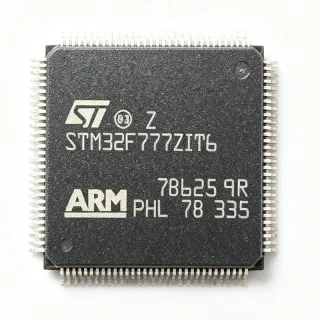
MK60FN1M0VLQ12 - K60 120MHz Cortex-M4F 1MB Flash MCU | NXP
MPN: MK60FN1M0VLQ12 ✓ 啟用中MK60FN1M0VLQ12 概覽
A 32-bit microcontroller (MCU) is a single-chip computer that integrates a CPU, peripherals, memory, and interface controllers into one package, enabling embedded intelligence in everything from appliances to automotive ECUs. The Cortex-M4F core adds a single-precision FPU and DSP extensions, while the Kinetis K-series sits within NXP's broader ARM Cortex-M portfolio targeting scalable performance from 50 MHz ultra-low-power variants up to multi-gigahertz crossover MCUs. This places the MK60FN1M0VLQ12 in the mid-performance tier optimized for mixed control + connectivity workloads.
Key features of the MK60FN1M0VLQ12 include 1 MB Flash, 128 KB SRAM, 120 MHz maximum CPU frequency, supply voltage range of 1.71 V to 3.6 V, operating temperature range of -40C to +105C, integrated full-speed plus high-speed USB OTG, 10/100 Mbps Ethernet MAC with IEEE 1588, and a 16-bit SAR ADC. The LQFP-144 (20x20 mm) package exposes up to 100 GPIO pins, multiple serial peripherals (UART, SPI, I2C), an SDHC controller, and a flexible FlexTimer/PWM subsystem.
Architecturally, the MK60FN1M0VLQ12 uses the Cortex-M4F core with NVIC, DSP instructions, and an FPU, paired with crossbar switch and AIPS-Lite peripheral bridges that allow simultaneous DMA-driven peripheral access without stalling the core. Hardware encryption is supported through on-chip acceleration, enabling secure boot, AES, and hashing without offloading to software.
Typical applications include industrial Ethernet control nodes, USB audio interfaces, point-of-sale terminals, smart energy metering, building automation gateways, and motion-control drives. The combination of Ethernet plus dual USB plus 1 MB Flash is particularly well-matched to gateways that aggregate multiple fieldbus segments.
When designing with this MCU, verify that the supply rail respects the 1.71 V to 3.6 V range and use low-ESR decoupling at each VDD/VSS pair. For USB high-speed operation, the dedicated PLL must be configured before enabling the HS controller; ignoring this prevents USB enumeration. This page synthesizes distributor pricing, drop-in alternatives, and practical design notes not found in the manufacturer datasheet alone.
直接替換替代品,適用於 MK60FN1M0VLQ12 — 相同封裝,腳位對腳位相容。需重新設計 PCB 的不同封裝零件不列入。
此系列的變體
與下列產品可直接替換的同系列型號: MK60FN1M0VLQ12 (相同外形與佔位) — 差異在於 Package, ADC, Operating Temperature Range, USB, DAC.
MK60FN1M0VLQ15
✅ 直接替換📋 參考替代品(不在目錄中)
MK60FX512VLQ12
✅ 直接替換📋 參考替代品(不在目錄中)
MK60FX512VLQ15
✅ 直接替換📋 參考替代品(不在目錄中)
MK66FN2M0VLQ18
✅ 直接替換聯絡詢價
查看資料表 →MK60DN512VMD10
✅ 直接替換聯絡詢價
查看資料表 →MK60FN1M0VLQ12 最大額定值與電氣特性
| Core | ARM Cortex-M4F with FPU and DSP |
| Maximum CPU Frequency | 120 MHz |
| Program Flash Memory | 1 MB (1024 KB) |
| SRAM | 128 KB |
| Supply Voltage Range | 1.71 V to 3.6 V |
| 工作溫度範圍 | -40C to +105C (V suffix) |
| 封裝 | LQFP-144 (20x20 mm) |
| 腳位數 | 144 |
| USB Controllers | USB 2.0 FS OTG + HS OTG (dual) |
| Ethernet MAC | 10/100 Mbps with IEEE 1588 |
| Hardware Encryption | Yes (on-chip acceleration) |
| ADC | 16-bit SAR ADC |
| 安裝類型 | Surface Mount |
| 生命週期狀態 | Active |
| RoHS 狀態 | Compliant |
MK60FN1M0VLQ12 腳位配置
| 腳位 1 | PTE0 — Port E GPIO / UART1_CTS |
| 腳位 2 | PTE1 — Port E GPIO / UART1_RTS |
| 腳位 3 | PTE2 — Port E GPIO / SPI1_SOUT |
| 腳位 4 | PTE3 — Port E GPIO / SPI1_SIN |
| 腳位 5 | PTE4 — Port E GPIO / SPI1_PCS0 |
| 腳位 6 | PTE5 — Port E GPIO |
| 腳位 7 | PTE6 — Port E GPIO |
| 腳位 8 | VSS — Ground |
| 腳位 9 | USB0_DP — USB FS OTG data plus |
| 腳位 10 | USB0_DM — USB FS OTG data minus |
| 腳位 11 | VDD — Supply voltage (3.3 V typical) |
| 腳位 12 | VSS — Ground |
| 腳位 13 | USB1_DP — USB HS OTG data plus |
| 腳位 14 | USB1_DM — USB HS OTG data minus |
| 腳位 15 | VREGIN — Voltage regulator input |
| 腳位 16 | VREGOUT — Voltage regulator output (1.2 V core) |
| 腳位 17 | VDD — Supply voltage |
| 腳位 18 | VSS — Ground |
| 腳位 19 | PTA0 — Port A GPIO / JTAG_TCLK |
| 腳位 20 | PTA1 — Port A GPIO / JTAG_TDI |
| 腳位 21 | PTA2 — Port A GPIO / JTAG_TDO |
| 腳位 22 | PTA3 — Port A GPIO / JTAG_TMS |
| 腳位 23 | PTA4 — Port A GPIO / NMI_b |
| 腳位 24 | PTA5 — Port A GPIO / Reset_b |
| 腳位 25 | PTA6 — Port A GPIO |
| 腳位 26 | PTA7 — Port A GPIO |
| 腳位 27 | PTB0 — Port B GPIO / ADC0_SE0 |
| 腳位 28 | PTB1 — Port B GPIO / ADC0_SE1 |
| 腳位 29 | PTB2 — Port B GPIO / ADC0_SE2 |
| 腳位 30 | PTB3 — Port B GPIO / ADC0_SE3 |
| 腳位 31 | PTB4 — Port B GPIO |
| 腳位 32 | PTB5 — Port B GPIO |
| 腳位 33 | PTB6 — Port B GPIO |
| 腳位 34 | PTB7 — Port B GPIO |
| 腳位 35 | PTC0 — Port C GPIO |
| 腳位 36 | PTC1 — Port C GPIO |
| 腳位 37 | PTC2 — Port C GPIO |
| 腳位 38 | PTC3 — Port C GPIO |
| 腳位 39 | PTC4 — Port C GPIO |
| 腳位 40 | PTC5 — Port C GPIO |
| 腳位 41 | PTC6 — Port C GPIO |
| 腳位 42 | PTC7 — Port C GPIO |
| 腳位 43 | PTD0 — Port D GPIO |
| 腳位 44 | PTD1 — Port D GPIO |
| 腳位 45 | PTD2 — Port D GPIO |
| 腳位 46 | PTD3 — Port D GPIO |
| 腳位 47 | PTD4 — Port D GPIO |
| 腳位 48 | PTD5 — Port D GPIO |
| 腳位 49 | PTD6 — Port D GPIO |
| 腳位 50 | PTD7 — Port D GPIO |
| 腳位 51 | PTE7 — Port E GPIO |
| 腳位 52 | PTE8 — Port E GPIO |
| 腳位 53 | PTE9 — Port E GPIO |
| 腳位 54 | PTE10 — Port E GPIO |
| 腳位 55 | PTE11 — Port E GPIO |
| 腳位 56 | PTE12 — Port E GPIO |
| 腳位 57 | PTE13 — Port E GPIO |
| 腳位 58 | PTE14 — Port E GPIO |
| 腳位 59 | PTE15 — Port E GPIO |
| 腳位 60 | PTF0 — Port F GPIO |
| 腳位 61 | PTF1 — Port F GPIO |
| 腳位 62 | PTF2 — Port F GPIO |
| 腳位 63 | PTF3 — Port F GPIO |
| 腳位 64 | PTF4 — Port F GPIO |
| 腳位 65 | PTF5 — Port F GPIO |
| 腳位 66 | PTF6 — Port F GPIO |
| 腳位 67 | PTF7 — Port F GPIO |
| 腳位 68 | PTG0 — Port G GPIO |
| 腳位 69 | PTG1 — Port G GPIO |
| 腳位 70 | PTG2 — Port G GPIO |
| 腳位 71 | PTG3 — Port G GPIO |
| 腳位 72 | PTG4 — Port G GPIO |
| 腳位 73 | PTG5 — Port G GPIO |
| 腳位 74 | PTG6 — Port G GPIO |
| 腳位 75 | PTG7 — Port G GPIO |
| 腳位 76 | PTH0 — Port H GPIO |
| 腳位 77 | PTH1 — Port H GPIO |
| 腳位 78 | PTH2 — Port H GPIO |
| 腳位 79 | PTH3 — Port H GPIO |
| 腳位 80 | PTH4 — Port H GPIO |
| 腳位 81 | PTH5 — Port H GPIO |
| 腳位 82 | PTH6 — Port H GPIO |
| 腳位 83 | PTH7 — Port H GPIO |
| 腳位 84 | PTI0 — Port I GPIO |
| 腳位 85 | PTI1 — Port I GPIO |
| 腳位 86 | PTI2 — Port I GPIO |
| 腳位 87 | PTI3 — Port I GPIO |
| 腳位 88 | PTI4 — Port I GPIO |
| 腳位 89 | PTI5 — Port I GPIO |
| 腳位 90 | PTI6 — Port I GPIO |
| 腳位 91 | PTI7 — Port I GPIO |
| 腳位 92 | NC — Not connected |
| 腳位 93 | NC — Not connected |
| 腳位 94 | NC — Not connected |
| 腳位 95 | NC — Not connected |
| 腳位 96 | NC — Not connected |
| 腳位 97 | NC — Not connected |
| 腳位 98 | NC — Not connected |
| 腳位 99 | NC — Not connected |
| 腳位 100 | NC — Not connected |
| 腳位 101 | NC — Not connected |
| 腳位 102 | NC — Not connected |
| 腳位 103 | NC — Not connected |
| 腳位 104 | NC — Not connected |
| 腳位 105 | NC — Not connected |
| 腳位 106 | NC — Not connected |
| 腳位 107 | NC — Not connected |
| 腳位 108 | NC — Not connected |
| 腳位 109 | NC — Not connected |
| 腳位 110 | NC — Not connected |
| 腳位 111 | NC — Not connected |
| 腳位 112 | NC — Not connected |
| 腳位 113 | NC — Not connected |
| 腳位 114 | NC — Not connected |
| 腳位 115 | NC — Not connected |
| 腳位 116 | NC — Not connected |
| 腳位 117 | NC — Not connected |
| 腳位 118 | NC — Not connected |
| 腳位 119 | NC — Not connected |
| 腳位 120 | NC — Not connected |
| 腳位 121 | NC — Not connected |
| 腳位 122 | NC — Not connected |
| 腳位 123 | NC — Not connected |
| 腳位 124 | NC — Not connected |
| 腳位 125 | NC — Not connected |
| 腳位 126 | NC — Not connected |
| 腳位 127 | NC — Not connected |
| 腳位 128 | NC — Not connected |
| 腳位 129 | NC — Not connected |
| 腳位 130 | NC — Not connected |
| 腳位 131 | NC — Not connected |
| 腳位 132 | NC — Not connected |
| 腳位 133 | NC — Not connected |
| 腳位 134 | NC — Not connected |
| 腳位 135 | NC — Not connected |
| 腳位 136 | NC — Not connected |
| 腳位 137 | NC — Not connected |
| 腳位 138 | NC — Not connected |
| 腳位 139 | NC — Not connected |
| 腳位 140 | NC — Not connected |
| 腳位 141 | NC — Not connected |
| 腳位 142 | NC — Not connected |
| 腳位 143 | NC — Not connected |
| 腳位 144 | EP — Exposed pad - connect to ground |
典型應用
MK60FN1M0VLQ12 適用於 7 應用s: Industrial Ethernet Control Nodes, USB Audio Interfaces, Point-of-Sale Terminals, Smart Energy Metering, Building Automation Gateways, Motion Control Drives, Connected Medical Device Controllers.
Industrial Ethernet Control Nodes
The MK60FN1M0VLQ12 integrates a 10/100 Mbps Ethernet MAC with IEEE 1588 precision-time protocol support alongside a Cortex-M4F DSP-capable core at 120 MHz, making it well-suited for industrial Ethernet slaves and gateways that require deterministic latency on EtherNet/IP or PROFINET-style networks. The 1 MB Flash holds a TCP/IP stack plus application firmware, while the 128 KB SRAM supports multi-socket buffers. Engineers typically pair this MCU with an external PHY and a 50 MHz reference clock; unlike Cortex-M0 alternatives, the FPU and DSP extensions accelerate any on-node control-loop math.
推薦
USB Audio Interfaces
The MK60FN1M0VLQ12's dual USB 2.0 controllers (FS OTG plus HS OTG) plus its 120 MHz Cortex-M4F with FPU are aligned to USB audio class endpoints where high-bandwidth isochronous transfers and real-time DSP both run on the same chip. The 128 KB SRAM buffers multi-channel audio frames, while 1 MB Flash stores USB stack plus DSP effects. Designers typically place this MCU between a USB host and a CODEC such as the PCM1794A; unlike smaller Kinetis variants, this part avoids audio dropouts caused by USB bandwidth contention.
推薦
Point-of-Sale Terminals
The MK60FN1M0VLQ12's combination of Ethernet for back-office sync, dual USB for peripherals (card reader plus printer), and 1 MB Flash for payment-application firmware makes it a strong fit for compact POS terminals. Hardware encryption acceleration offloads AES and SHA from the Cortex-M4F, helping meet PCI transaction latency targets. The 16-bit SAR ADC reads keypad or battery monitoring; the FPU accelerates total calculation. Power dissipation at 120 MHz with all peripherals active is moderate, allowing fanless enclosed designs.
推薦
Smart Energy Metering
The MK60FN1M0VLQ12 is well-suited to single-phase or multi-phase smart energy meters that require precise metrology plus a connected interface. The 16-bit ADC samples current and voltage waveforms, while the Cortex-M4F DSP extensions compute RMS and harmonics in real time; the FPU accelerates complex-power calculations. Ethernet or dual USB handles HAN/WAN reporting, and the 1 MB Flash stores logs and DLMS/COSEM stacks. Industrial temperature grade (-40C to +105C) supports outdoor cabinet mounting.
推薦
Building Automation Gateways
The MK60FN1M0VLQ12 acts as a building-automation gateway that aggregates multiple fieldbus segments (Modbus, BACnet, KNX over UART or SPI) and publishes to the cloud via Ethernet. Its 1 MB Flash accommodates multi-protocol stacks, the 128 KB SRAM handles concurrent message queues, and the Cortex-M4F DSP accelerates any local control logic. The dual USB enables Wi-Fi or cellular dongle backup links; unlike Cortex-M0 gateways, the FPU handles encryption acceleration and signal processing in parallel.
推薦
Motion Control Drives
The MK60FN1M0VLQ12's FlexTimer/PWM subsystem, 120 MHz Cortex-M4F DSP, and FPU make it a fit for low-to-mid-power motion control drives that require fast current-loop computation. The 16-bit ADC samples phase currents, the FPU executes field-oriented control algorithms at sub-10 us loop times, and the Ethernet MAC streams drive telemetry to a supervisory controller. The 1 MB Flash holds application plus safety logic; the 144-LQFP exposes enough GPIO for encoder, hall sensor, and PWM channels.
推薦
Connected Medical Device Controllers
The MK60FN1M0VLQ12 serves as a connected medical-device controller where Ethernet or USB enables clinician tablets while the Cortex-M4F DSP and FPU handle real-time signal processing from the analog front end. The 1 MB Flash stores firmware plus safety logs, the 128 KB SRAM buffers sample streams, and hardware encryption protects patient data in transit. Unlike Cortex-M0 parts, the M4F core runs FFT and filter pipelines for biosignal processing. Industrial temperature grade supports bedside equipment environments.
推薦
推薦產品摘要
工程參考資料,適用於 MK60FN1M0VLQ12 — 比較、設計指引及合規資訊。
選型指南
與替代品比較
| 參數 | 本產品 | MK60FN1M0VLQ15 | MK60FX512VLQ12 | MK60FX512VLQ15 | MK66FN2M0VLQ18 | MK60DN512VMD10 |
|---|---|---|---|---|---|---|
| Package | LQFP-144 (20x20 mm) | LQFP-144 (20x20 mm) - same | LQFP-144 (20x20 mm) - same | LQFP-144 (20x20 mm) - same | LQFP-144 (20x20 mm) - same | MAPBGA-144 - different footprint |
| Brand | NXP Semiconductors | NXP Semiconductors | NXP Semiconductors | NXP Semiconductors | NXP Semiconductors | NXP Semiconductors |
| Core | ARM Cortex-M4F | ARM Cortex-M4F | ARM Cortex-M4F | ARM Cortex-M4F | ARM Cortex-M4F | ARM Cortex-M4 |
| Maximum CPU Frequency | 120 MHz | 150 MHz | 120 MHz | 150 MHz | 180 MHz | 100 MHz |
| Flash Memory | 1 MB | 1 MB | 512 KB | 512 KB | 2 MB | 512 KB |
| SRAM | 128 KB | 128 KB | 128 KB | 128 KB | 256 KB | 128 KB |
| Supply Voltage | 1.71 V to 3.6 V | 1.71 V to 3.6 V | 1.71 V to 3.6 V | 1.71 V to 3.6 V | 1.71 V to 3.6 V | 1.71 V to 3.6 V |
| Operating Temperature | -40C to +105C | -40C to +105C | -40C to +105C | -40C to +105C | -40C to +105C | -40C to +105C |
主要差異化特點
- Dual USB 2.0 (FS + HS) in a single 144-LQFP (對比MK60FX512VLQ12)
- Pin-compatible upgrade to 180 MHz / 2 MB Flash / 256 KB SRAM (對比MK66FN2M0VLQ18)
- Same-package variant with 150 MHz core for higher DSP throughput (對比MK60FN1M0VLQ15)
- Industrial temperature grade standard (對比Commercial-only K-series MCUs)
設計說明
The MK60FN1M0VLQ12 requires a clean 3.3 V rail within 1.71 V to 3.6 V. Decouple each VDD pin with a 100 nF ceramic plus 4.7 uF bulk capacitor placed within 5 mm of the pin. The internal voltage regulator (VREGIN to VREGOUT) needs its own 1 uF plus 100 nF pair; do not share decoupling with VDD. For USB high-speed operation, the on-chip PLL requires stable VDD within 50 mV ripple; add a ferrite bead on noisy rails.
Use a 4-layer PCB with a continuous ground plane under the LQFP-144 footprint to provide thermal spreading and low-impedance returns. The exposed pad (EP) must be soldered to a 5x5 mm copper pad with thermal vias to inner ground planes. Route USB DP/DM traces as 90 ohm differential pairs with length matching within 150 mil. Keep the 50 MHz Ethernet reference clock trace short and shielded by ground on both sides.
Do not enable the USB HS controller before configuring the internal HS PLL - per NXP community guidance this prevents USB enumeration. Always wait for the PLL lock bit before switching the USB clock source. Also, when migrating from K60 to K66, do not assume identical peripheral addresses; the K66 USB HS module has register differences that require firmware updates for HS operation, while FS USB remains drop-in compatible.
Estimated: at 120 MHz core and full peripheral activity, the MK60FN1M0VLQ12 typical core current is around 35 mA at 3.3 V plus I/O drive. The LQFP-144 has a theta_JA near 40 C/W on a 4-layer board, so junction temperature rise at 25C ambient is approximately 5 C. Industrial temperature parts (V suffix) are specified to +105C and need at least a 2 oz copper pour under the exposed pad for thermal relief. Always verify thermal performance in your enclosure.
合規資訊
RoHS compliant per NXP product page. Not AEC-Q100 qualified - this is an industrial-grade MCU, not automotive. Reach and conflict-minerals compliance per NXP standard declarations. Halogen-free status not explicitly stated in retrieved data.