Texas Instruments

TPS7A4701RGWR - 1A, 36V Ultra-Low Noise LDO | Texas Instruments

MPN: TPS7A4701RGWR ✓ 啟用中
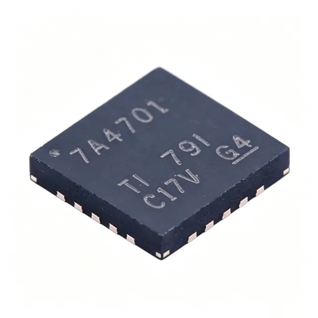
1.4 V to 34 V Vdss 1 A Id 20-VQFN (5x5 mm) with exposed pad Package
MOQ: 1 |

TPS7A4701RGWR 概覽

The Texas Instruments TPS7A4701RGWR is a 1 A ultra-low-noise LDO linear regulator with 4.17 uVRMS output noise, a 3 V to 36 V input range, and an adjustable output from 1.4 V to 34 V, housed in a 20-pin VQFN (RGW) 5x5 mm package with exposed thermal pad.

An LDO (low-dropout) linear regulator is a type of voltage regulator that maintains a stable output voltage even when the input voltage is only marginally higher than the output. Within the power management IC hierarchy, LDOs sit downstream of switching converters, providing the final, noise-free regulation stage that sensitive analog loads require. Unlike DC-DC converters, LDOs add no switching ripple, which is why they dominate RF, audio, and precision instrumentation power rails.

Key features include 4.17 uVRMS output noise over the 20 Hz to 100 kHz bandwidth, 1 A output capability, and a low dropout voltage of approximately 307 mV, per the TI TPS7A47 datasheet. The TPS7A4701 variant offers an externally adjustable output via a feedback pin, while the sibling TPS7A4700 uses a PCB-programmable scheme requiring no external resistors. An enable pin supports power sequencing in multi-rail systems.

The device is built on bipolar technology, chosen specifically for high-accuracy, high-precision instrumentation where clean rails maximize system performance. According to TI, the TPS7A47 family is optimized for powering operational amplifiers, ADCs, DACs, and other high-performance analog circuitry, where its high power-supply rejection suppresses upstream switching-converter ripple.

Typical applications include RF PLL/VCO power supplies in transceivers, audio DAC/ADC analog rails, precision test-and-measurement instrumentation, and industrial systems running from 24 V buses where the 36 V input rating provides ample headroom.

A key design consideration is thermal budget: at large input-to-output differentials and full 1 A load, dissipation can reach several watts, so the exposed pad must be soldered to a generous copper pour. The NR/SS capacitor also sets soft-start and noise-reduction bandwidth and should not be omitted.

This page synthesizes distributor pricing (as of 2026-09-01), drop-in alternatives, and practical design notes not found in the manufacturer datasheet.

直接替換替代品,適用於 TPS7A4701RGWR — 相同封裝,腳位對腳位相容。需重新設計 PCB 的不同封裝零件不列入。

此系列的變體

與下列產品可直接替換的同系列型號: TPS7A4701RGWR (相同外形與佔位) — 差異在於 Output Noise, Output Type, Output Voltage Range, Enable Pin, Input Voltage Range.

Texas Instruments
Output Noise: 4.17 uVRMS (20 Hz to 100 kHz)
Output Type: Positive, adjustable (ANY-OUT programmable)
Output Voltage Range: 1.4 V to 20.5 V (ANY-OUT via PCB layout)
比較對象 TPS7A4701RGWR →
Texas Instruments
Output Noise: 4.2 uVRMS (20 Hz to 100 kHz)
Output Type: Adjustable/Programmable
Output Voltage Range: 1.4 V to 34 V (adjustable), up to 20.5 V (PCB-programmable)
比較對象 TPS7A4701RGWR →

TPS7A4700RGWR

✅ 直接替換
Texas Instruments
📦 20-VQFN (5x5)
Positive, adjustable (ANY-OUT programmable) · 1.4 V to 20.5 V (ANY-OUT via PCB layout) · 1 A · 3 V to 36 V · 4.17 uVRMS (20 Hz to 100 kHz)

聯絡詢價

查看資料表 →

TPS7A4701QRGWRQ1

✅ 直接替換
Texas Instruments
📦 20-VQFN (5x5)
Adjustable/Programmable · 1.4 V to 34 V (adjustable), up to 20.5 V (PCB-programmable) · 1 A · Up to 35 V · 4.2 uVRMS (20 Hz to 100 kHz) · LDO (Low-Dropout Linear Regulator) · 1 · Positive

聯絡詢價

查看資料表 →

TPS7A3301RGWR

✅ 直接替換
📦 20-VQFN (5x5)
Negative-output LDO (-1.4 V to -36 V class) in same RGW footprint; same 1 A current class but opposite polarity - complementary rail part, not a positive-rail substitute

📋 參考替代品(不在目錄中)

TPS7A4701RGWR 最大額定值與電氣特性

輸出類型 Positive Adjustable, 1 channel
輸出電壓範圍 1.4 V to 34 V
最大輸出電流 1 A
輸入電壓範圍 3 V to 36 V
壓降電壓 307 mV
輸出雜訊 4.17 uVRMS
Technology Bipolar
封裝 20-VQFN (5x5 mm) with exposed pad
安裝類型 Surface Mount
致能腳位 Yes
Product Family TPS7A47 RF LDO
Marking Code 7A4701
Packaging Tape & Reel (T/R)

TPS7A4701RGWR 20-vqfn (5x5 mm) with exposed pad 腳位配置指南

TPS7A4701RGWR(20-vqfn (5x5 mm) with exposed pad 封裝)的腳位配置。 此功率元件具有閘極、汲極與源極端子。對於非極性封裝,請參閱製造商資料表以取得確切的第 1 腳方向與佈局詳細資訊。常見應用包括電源設計、馬達驅動與負載切換。

TPS7A4701RGWR 的 20-vqfn (5x5 mm) with exposed pad 封裝腳位圖

無詳細腳位定義資料: TPS7A4701RGWR.

請參閱 資料表 以查看完整腳位配置。

典型應用

TPS7A4701RGWR 適用於 6 應用s: RF PLL/VCO Power Supply, Precision Test and Measurement Instrumentation, High-End Audio DAC and ADC Supplies, Industrial 24V Bus Regulation, Precision ADC/DAC Reference Buffering Chains, Multi-Rail Processor and FPGA Analog Rails.

🌐

RF PLL/VCO Power Supply

RF synthesizers place extreme demands on supply noise: VCO pushing figures mean that even microvolts of rail noise convert directly into phase noise, degrading integrated jitter and EVM. The TPS7A4701RGWR addresses this with 4.17 uVRMS output noise (20 Hz to 100 kHz) and TI-classified RF LDO performance built on bipolar technology. It is typically placed after a switching pre-regulator, where its ripple rejection cleans the 5 V or 3.3 V rail feeding the PLL charge pump and VCO tuning supply. Because the part tolerates up to 36 V input, it can also regulate directly from higher intermediate rails. Designers should keep the NR/SS capacitor close to the pin to preserve the low-noise bandwidth and route the VCO supply as a star branch off the LDO output.

🔧

Precision Test and Measurement Instrumentation

Bench instruments, digitizers, and calibration hardware require analog rails with negligible noise so that the instrument itself does not become the dominant error source. According to TI, the TPS7A47 family is designed with bipolar technology primarily for high-accuracy, high-precision instrumentation where clean voltage rails maximize system performance. The TPS7A4701RGWR supplies op-amp and ADC stages from its 1.4 V to 34 V adjustable output, sourcing up to 1 A for multi-channel analog front ends. Its 36 V maximum input supports direct regulation from industrial supplies used in rack equipment. Thermal design matters: the exposed VQFN-20 pad must bond to a solid ground pour, and at large VIN-VOUT differentials the dissipation budget should be verified before layout release.

🎧

High-End Audio DAC and ADC Supplies

Audio DAC and ADC analog supplies directly influence dynamic range and THD+N; ripple or noise on AVDD appears as spurious tones in the output spectrum. The TPS7A4701RGWR's 4.17 uVRMS noise floor and bipolar architecture make it well suited to powering DAC analog rails and op-amp I/V conversion stages. Placed between a 12 V or 15 V supply and the DAC AVDD pin with 10 uF local ceramics, it adds no switching artifacts. The 1 A rating covers high-current DACs and their analog output stages. Compared with generic LDOs, the key benefit is noise floor; the trade-off is higher quiescent dissipation at large input-output deltas, so headroom should be minimized while maintaining the ~307 mV dropout margin.

🏭

Industrial 24V Bus Regulation

Industrial control and sensor-excitation systems commonly run from 24 V buses with transient excursions toward 30 V or more. The TPS7A4701RGWR's 3 V to 36 V input range provides direct headroom for these rails, eliminating an intermediate switching stage when load currents are moderate. It can generate clean 5 V or adjustable analog rails for transmitters, ADC front ends, and reference circuits on PLC I/O cards. Because dropout is approximately 307 mV at load, the part also works in post-regulation roles after a buck converter reduces the bus. Designers must account for worst-case dissipation at full differential - at 24 V input and 5 V output the device dissipates heavily at 1 A, so copper area or derating is essential.

📺

Precision ADC/DAC Reference Buffering Chains

High-resolution converters are only as good as their supplies and references: PSR of an ADC falls with frequency, so high-frequency supply ripple leaks into conversion results. The TPS7A4701RGWR provides a quiet rail for the reference buffer amplifier and analog supply pins of 18- to 24-bit converters, with the 4.17 uVRMS noise figure translating into a sub-LSB noise contribution at typical reference levels. The adjustable output via the FB pin lets designers tune the rail to exactly the converter's recommended AVDD. Layout discipline - short, wide output traces and local 10 uF plus 0.1 uF decoupling - preserves the datasheet noise performance in the final assembly.

🖥️

Multi-Rail Processor and FPGA Analog Rails

FPGAs and SoCs mix noisy core rails with noise-sensitive PLL, transceiver, and analog supplied rails. The TPS7A4701RGWR's enable pin supports sequenced power-up of the quiet rails after core supplies, satisfying FPGA power-supply sequencing requirements. Post-regulating a switching converter output down to the gigabit transceiver AVDD rail with this LDO suppresses switching residue and lowers jitter. The 1 A capability covers multiple transceiver banks, and the 36 V input allows the part to sit on unconditioned backplane supplies. Use the FB divider with 1%-tolerance resistors, and keep the soft-start NR/SS capacitor sized so inrush does not trip upstream protection.

What is the input voltage range of TPS7A4701RGWR?
The TPS7A4701RGWR operates from an input voltage of 3 V to 36 V. According to the Texas Instruments TPS7A47 product page and distributor listings (Mouser describes it as a 36 V, 1 A, 4.17 uVRMS RF LDO), this wide input range allows direct connection to industrial 24 V rails with headroom, while the dropout voltage is approximately 307 mV per the TI datasheet.
What is the output noise of TPS7A4701RGWR?
The TPS7A4701RGWR has an output noise of 4.17 uVRMS (approximately 4 uVRMS per TI's family description) over the 20 Hz to 100 kHz bandwidth. This ultra-low-noise figure is the key reason the part is chosen for RF PLL/VCO supplies, audio DAC rails, and precision ADC references, where noise on the power rail directly degrades signal-chain dynamic range.
What is the maximum output current of TPS7A4701RGWR?
The TPS7A4701RGWR can source up to 1 A of continuous load current. Per the TI TPS7A47 datasheet, the family is described as a +36 V, ultralow-noise (4 uVRMS) low-dropout regulator capable of sourcing a 1 A load, making it suitable for powering entire analog signal-chain sections rather than just single low-power blocks.
What is the difference between TPS7A4701RGWR and TPS7A4700RGWR?
The TPS7A4701 has an externally adjustable output via a feedback pin, while the TPS7A4700 output voltage is programmed by a PCB layout scheme requiring no external resistors or feed-forward capacitors. Both share the same 36 V, 1 A, 4 uVRMS performance and the same VQFN-20 package, so they are pin-compatible drop-in alternatives; choose the 4701 when you need resistor-adjustable output flexibility.
Can TPS7A3301RGWR replace TPS7A4701RGWR?
Only for negative-rail designs. The TPS7A3301 shares the same VQFN-20 (RGW) footprint and is pin-compatible, but it is a negative LDO outputting -1.4 V to approximately -36 V rather than a positive 1.4 V to 34 V regulator. TI designed the two as complementary parts for symmetric supplies; it cannot substitute for the TPS7A4701 in a positive-rail application.
What is the best drop-in replacement for TPS7A4701RGWR?
The best drop-in replacement is the TPS7A4700RGWR, which is pin-compatible in the same 20-pin VQFN (RGW) package with identical 1 A, 36 V, 4 uVRMS performance; the only change is the output-voltage programming method. For automotive applications, the TPS7A4701QRGWRQ1 offers the same die in a Q1-qualified variant. No cross-brand pin-compatible equivalent was found in verified distributor cross-reference data.
Is TPS7A4701RGWR suitable for powering RF VCOs and PLLs?
Yes. Texas Instruments classifies the TPS7A47 as an RF LDO, with 4.17 uVRMS output noise and bipolar technology specifically targeting RF signal chains. VCO phase noise is highly sensitive to supply noise, so the ultra-low noise floor and high ripple rejection of this LDO directly reduce integrated phase noise in PLL/VCO synthesizer supplies used in transceivers and test equipment.
Where can I buy TPS7A4701RGWR and what does it cost?
TPS7A4701RGWR is available from major distributors including DigiKey, Mouser, Arrow, and LCSC. As of 2026-09-01, LCSC lists the part in stock starting at approximately $3.25 per unit (single-unit price); volume pricing typically steps down in the $2 to $3 range at 100 to 1000 pieces. XAIPART offers tiered pricing - see the pricing table on this page for exact quantity breaks.
Is TPS7A4701RGWR in stock?
Yes, TPS7A4701RGWR is broadly stocked. As of 2026-09-01, DigiKey lists the part with same-day shipping, LCSC shows it in stock (price from $3.2467), and Mouser and Arrow also list inventory. Availability is generally healthy because the device is an active TI product, but always confirm real-time stock on the distributor page before committing to a production schedule.
Where to download the TPS7A4701RGWR datasheet PDF?
The official datasheet is available on Texas Instruments' website at ti.com/lit/ds/symlink/tps7a4701.pdf, which serves the TPS7A470x 36-V, 1-A, 4-uVRMS RF LDO voltage regulator datasheet. Copies are also hosted on distributor sites such as DigiKey, Mouser, Arrow, and aggregator sites like alldatasheet.com (31-page document per their listing). Always prefer the TI.com version to ensure you have the latest revision.
Does TPS7A4701RGWR require a heatsink at 1A load?
It depends on the input-to-output differential. Estimated: at VIN = 12 V, VOUT = 5 V, and 1 A load, dissipation is about 7 W, which the VQFN-20 package cannot handle without substantial heatsinking - a large copper pour or airflow is mandatory. At a 6 V to 5 V conversion (1 W dissipation), the exposed thermal pad soldered to a 1-2 square inch ground pour is typically sufficient. Always calculate junction temperature against the theta-JA in the TI datasheet for your exact conditions.
TPS7A4701RGWR vs TPS7A8300RGRR - which is better for precision analog?
For precision analog, the choice depends on input voltage. The TPS7A4701RGWR supports up to 36 V input with 4.17 uVRMS noise, making it the right choice for 24 V industrial buses and high-voltage rails. The TPS7A8300 offers lower noise (typically ~2 uVRMS with NR cap) and lower dropout but a lower maximum input voltage. Choose the TPS7A4701 when input headroom above ~20 V or rail robustness dominates; choose the TPS7A8300 for low-voltage, lowest-noise point-of-load needs.
When should I choose TPS7A4701 over TPS7A4700?
Choose the TPS7A4701 when you need resistor-adjustable output voltage, when the output may change during design iterations, or when a single PCB layout must support multiple voltage options. Choose the TPS7A4700 when the voltage is fixed and you want to minimize component count, because the TPS7A4700 programs the output via PCB trace pattern with no external resistors or feed-forward capacitors. Both are electrically identical otherwise and share the VQFN-20 footprint.
What is the best ADI equivalent for TPS7A4701RGWR?
No verified cross-brand pin-compatible equivalent for the TPS7A4701RGWR was found in the distributor cross-reference data used for this page. Analog Devices LT3045-class ultra-low-noise LDOs are parametrically similar (ultra-low noise, ~500 mA, up to 20 V input) but use different packages and pinouts, so they are not drop-in replacements and would require PCB rework. Any substitution should be validated against footprint and pinout before layout release.
What are the key specifications of TPS7A4701RGWR that engineers should know?
The Texas Instruments TPS7A4701RGWR is a positive adjustable LDO regulator with a 3 V to 36 V input range, 1.4 V to 34 V adjustable output, 1 A output current, 307 mV dropout voltage, and 4.17 uVRMS output noise, in a 20-pin VQFN 5x5 mm exposed-pad package. It is built on bipolar technology for precision instrumentation and RF applications, includes an enable pin for sequencing, and is an active, RoHS-relevant TI product stocked at DigiKey, Mouser, Arrow, and LCSC as of 2026-09-01.
Is TPS7A4701RGWR the same as TPS7A4701RGWT?
Electrically yes - only the packaging format differs. Per FindIC comparison data, the TPS7A4701RGWT is the same die with identical electrical specifications (3 V to 36 V input, 307 mV dropout, 1.4 V to 34 V output, VQFN-20); the RGWR suffix denotes tape-and-reel packing while RGWT denotes a smaller-reel tape option. Either may be used interchangeably on the same PCB; choose based on assembly-volume requirements.
Is TPS7A4701RGWR RoHS compliant and still in production?
The TPS7A4701RGWR is an active TI product and is available across all major distributors as of 2026-09-01, indicating full production status. Texas Instruments' standard VQFN-20 parts of this generation are lead-free and RoHS-compliant; confirm the exact RoHS/REACH certificate on the TI product page for your build documentation. The device is not marketed as AEC-Q100 qualified - use the TPS7A4701QRGWRQ1 variant for automotive requirements.

工程參考資料,適用於 TPS7A4701RGWR — 比較、設計指引及合規資訊。

選型指南

Choose the TPS7A4701RGWR when you need an ultra-low-noise (4.17 uVRMS) positive LDO with wide 36 V input headroom and resistor-adjustable output up to 34 V - typical for RF PLL/VCO rails, precision instrumentation, and 24 V industrial buses. Choose TPS7A4700RGWR for the same performance with fewer external components when the output voltage is fixed below 20.5 V and will not change. Choose TPS7A4701QRGWRQ1 for automotive programs requiring the Q1-qualified variant of the identical die. Choose TPS7A3301 only for negative complementary rails - it is footprint-compatible but opposite polarity. If input voltage is below about 20 V and absolute lowest noise matters more than VIN range, consider lower-noise alternatives such as the TPS7A8300, accepting that it is not pin-compatible and requires PCB rework. All listed drop-in options share the 20-pin VQFN (5x5) footprint.

與替代品比較

參數 本產品 TPS7A4700RGWR TPS7A4701QRGWRQ1 TPS7A3301RGWR
Package 20-VQFN (5x5) exposed pad 20-VQFN (5x5) - same 20-VQFN (5x5) - same 20-VQFN (5x5) - same
Brand Texas Instruments Texas Instruments Texas Instruments Texas Instruments
Output Current 1 A 1 A 1 A 1 A
Output Polarity / Range Positive, 1.4 V to 34 V adjustable Positive, PCB-programmed up to 20.5 V Positive, 1.4 V to 34 V adjustable Negative, -1.4 V to about -36 V
Automotive Qualification No No Yes (Q1 variant) No

主要差異化特點

  • Resistor-adjustable output up to 34 V (對比TPS7A4700RGWR)
  • 36 V input tolerance on a low-noise LDO (對比TPS7A8300RGRR)
  • Standard (non-automotive) cost position (對比TPS7A4701QRGWRQ1)

設計說明

Estimated: at VIN = 12 V, VOUT = 5 V, and full 1 A load, dissipation reaches about 7 W - far beyond what the VQFN-20 package can dissipate with a nominal footprint, so junction temperature will exceed limits without major copper area or airflow. For high-differential designs, either reduce load current, add a switching pre-regulator, or verify junction temperature using the theta-JA values in the TI datasheet for your specific PCB stackup. Solder the exposed thermal pad to a minimum 1-2 square inch solid ground pour with thermal vias.

Place a 10 uF ceramic input capacitor and 10 uF output capacitor within a few millimeters of the IN and OUT pins, and add a 0.1 uF capacitor in parallel on the output for high-frequency decoupling. The FB divider resistors should be 1% tolerance or better to preserve output accuracy, and their midpoint trace to the FB pin should be short and away from switching nodes. Keep the NR/SS capacitor loop tight - it sets the noise-reduction bandwidth that delivers the 4.17 uVRMS figure.

Do not exceed the 36 V absolute maximum input, and beware inductive spikes on long industrial wiring - input TVS protection is prudent on 24 V bus applications. Do not substitute the TPS7A3301 (negative LDO) for this part on positive rails despite the identical footprint. When replacing a TPS7A4700 with a TPS7A4701 on an existing PCB, the TPS7A4700's PCB-programmed output pattern must be disconnected and the FB network added; verify before reflow.

Use the enable pin for rail sequencing in multi-supply systems such as FPGA or ADC power trees, releasing the analog rail after the core supply is stable. The soft-start behavior governed by the NR/SS capacitor limits inrush into large output capacitor banks; size output capacitance accordingly to avoid tripping upstream current limits during startup.

合規資訊

RoHS
Unknown
REACH
Unknown
AEC-Q100
Not Qualified
無鉛
Unknown
無鹵
Unknown
衝突礦產
Unknown

Standard TI catalog part, not marketed as AEC-Q100; the TPS7A4701QRGWRQ1 variant serves automotive requirements. RoHS/REACH certificates should be pulled from the TI product page for build documentation - values not present in the retrieved web data.

資料驗證日期: 2026-09-01 — 資料由 XAIPART 元件工程團隊驗證及整理

相關搜尋

TPS7A4701RGWR TPS7A4701 datasheet Texas Instruments TPS7A4701RGWR price ultra low noise LDO 1A 36V VQFN-20 low dropout regulator 4uVRMS TPS7A4701 RF VCO power supply TPS7A4701 vs TPS7A4700 difference TPS7A4701RGWR drop-in replacement buy TPS7A4701RGWR in stock what is the output noise of TPS7A4701RGWR TPS7A4701 pinout VQFN-20 best Analog Devices equivalent for TPS7A4701 TPS7A4701 audio DAC LDO regulator

相關元件與詞彙

Texas Instruments TPS7A4701RGWR TPS7A47 TPS7A4700RGWR TPS7A4701QRGWRQ1 TPS7A3301RGWR TPS7A8300RGRR LDO low-dropout regulator linear regulator voltage regulator power management IC output noise PSRR dropout voltage bipolar technology VQFN-20 QFN package family surface mount RF LDO PLL/VCO power supply audio DAC supply precision instrumentation tape and reel
相關技術指南
TPS7A4701RGWR: Complete Guide to TI's 1A, 35V Ultra-Low Noise LDO Regulator
TPS7A4701RGWR: TI's 1A ultra-low noise LDO with 4.17 uVrms noise, 72 dB PSRR, 3-35V input, VQFN-20. In stock, $3.2467 as of 2026-09-02.
6 分鐘閱讀
TPS7A4700RGWR: 36V 1A Ultralow-Noise LDO — Complete Engineer's Guide, Specs, and Alternatives
TPS7A4700RGWR: TI 36V-input, 1A LDO with 4.17 µVRMS noise, ANY-OUT programming 1.4–20.5V, VQFN-20. In stock now at XAIPART.
8 分鐘閱讀
快速報價 RFQ
請填寫完整詳細資料 — 我們的業務團隊將於 24 小時內回覆
料號 製造商 封裝 QTY 目標價格 小計
✓
報價已提交!

我們將於 24 小時內回覆您的電子郵件

1
詢價已提交
2
已收到報價
3
已下單
4
付款
5
已出貨
6
已送達
檢視詢價單詳情



