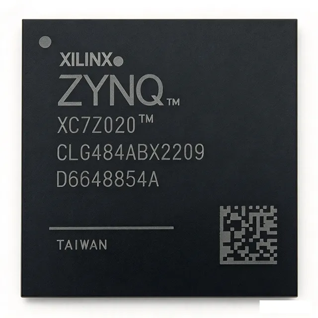
XC7Z020-1CLG484I - Zynq-7000 SoC 667MHz Dual ARM Cortex-A9 | AMD/Xilinx
MPN: XC7Z020-1CLG484I ✓ 啟用中| 數量 | 單價 | 小計 |
|---|---|---|
| 1 | $78.75 | $78.75 |
| 10 | $56.875 | $568.75 |
| 100 | $50.3125 | $5,031.25 |
| 500 | $48.125 | $24,062.50 |
| 1,000 | $45.9375 | $45,937.50 |
XC7Z020-1CLG484I 概覽
A SoC FPGA such as the Zynq-7000 is a single silicon device that fuses a hard processor subsystem (HSS) and a soft FPGA fabric. The processor subsystem runs software (Linux, RTOS, bare-metal), while the programmable logic provides hardware acceleration, custom I/O, and parallel data-path extensions. Zynq-7000 devices sit within the broader taxonomy of heterogeneous compute devices, alongside MPSoC and Versal Adaptive SoC families from AMD/Xilinx. This hybrid architecture is ideal for embedded systems that require both deterministic real-time control and high-throughput data processing.
Key features include dual ARM Cortex-A9 cores with NEON SIMD and single/double precision FPU, on-chip L1 caches (32 KB I-cache, 32 KB D-cache per core) and 512 KB L2 cache, integrated Memory Controller for DDR3/DDR3L/LPDDR2, dual USB 2.0 OTG, dual Gigabit Ethernet MACs, dual SD/SDIO controllers, and 2x UART, 2x SPI, 2x I2C peripheral interfaces. The integrated Artix-7 FPGA fabric includes 85K logic cells, 4.9 Mb block RAM, and 220 DSP slices.
The Zynq-7000 architecture uses a tightly coupled AXI interconnect between the PS and PL, allowing hardware-accelerated peripherals to communicate with the processor at high bandwidth with predictable latency. The CLG484 package exposes multiple high-performance (HP) and high-range (HR) I/O banks for DDR interfacing and general-purpose I/O.
Typical applications include industrial motor drives, machine vision, software-defined radio, ADAS driver assistance systems, medical imaging, and embedded vision. The wide temperature range and -1 speed grade make the XC7Z020-1CLG484I well suited for industrial control and factory automation.
When designing with this device, careful attention must be paid to PCB layout, power-rail sequencing, and DDR signal integrity. Use Vivado Design Suite and Vitis for hardware/software co-design, and refer to the official Zynq-7000 datasheet (DS187) and PCB design guide (UG933).
This page synthesizes distributor pricing, drop-in alternatives, and practical design notes not found in the manufacturer datasheet.
直接替換替代品,適用於 XC7Z020-1CLG484I — 相同封裝,腳位對腳位相容。需重新設計 PCB 的不同封裝零件不列入。
此系列的變體
與下列產品可直接替換的同系列型號: XC7Z020-1CLG484I (相同外形與佔位) — 差異在於 Logic Cells, Mounting Type, Package, Speed Grade.
快速比較工具 — 選擇替代零件進行並排比較:
XC7Z020-2CLG484I
✗ 缺貨
$49 / 單位
查看資料表 →XC7Z020-1CLG484C
📋 參考替代品(不在目錄中)
XC7Z020-1CLG400I
📋 參考替代品(不在目錄中)
XC7Z020-1CLG484I 最大額定值與電氣特性
| Family | Zynq-7000 All Programmable SoC |
| Device | XC7Z020 |
| Speed Grade | -1 |
| Processing System | Dual ARM Cortex-A9 MPCore |
| Max Processor Clock | 667 MHz |
| FPGA Fabric | Artix-7 |
| Logic Cells | 85K |
| Block RAM | 4.9 Mb |
| DSP Slices | 220 |
| 封裝 | 484-ball CSBGA (CLG484) 19x19 mm |
| Temperature Grade | Industrial (-40C to +100C) |
| L1 Cache (per core) | 32 KB I-cache + 32 KB D-cache |
| L2 Cache | 512 KB |
| 安裝類型 | Surface Mount (BGA) |
| RoHS 狀態 | Compliant |
XC7Z020-1CLG484I 484-ball csbga (clg484) 19x19 mm 腳位配置指南
XC7Z020-1CLG484I(484-ball csbga (clg484) 19x19 mm 封裝)的腳位配置。 此數位 IC 包含 GPIO、通訊介面(UART、SPI、I2C)與電源腳位。替代腳位功能與配置選項請參閱製造商資料表。對嵌入式系統設計與 PCB 佈局至關重要。

無詳細腳位定義資料: XC7Z020-1CLG484I.
請參閱 資料表 以查看完整腳位配置。
典型應用
XC7Z020-1CLG484I 適用於 6 應用s: Industrial Motor Control, Machine Vision Systems, Software-Defined Radio, Embedded IoT Gateways, Medical Imaging and Diagnostic Equipment, ADAS and Driver Assistance.
Industrial Motor Control
The XC7Z020-1CLG484I fits industrial motor control applications by combining a real-time capable ARM Cortex-A9 processor with hardware-accelerated FPGA fabric. The 667 MHz dual-core CPU handles motion-control algorithms and EtherCAT/EtherNet/IP stack processing, while the Artix-7 PL fabric implements custom PWM generators, encoder interfaces, and current-sampling logic with sub-microsecond latency. The 220 DSP slices accelerate Field-Oriented Control (FOC) and PID computations. The CLG484 package exposes sufficient HP/HR I/O banks for multi-axis servo drive designs.
推薦
Machine Vision Systems
The XC7Z020-1CLG484I fits machine vision systems where image acquisition, preprocessing, and inference must run on a single chip. The dual ARM Cortex-A9 cores run Linux with OpenCV or vendor SDKs, while the Artix-7 fabric implements hardware-accelerated image preprocessing (filtering, morphology, Bayer-to-RGB conversion) at line rates exceeding 200 MP/s. The integrated DDR3 controller supports high-bandwidth camera sensor data, and the 4.9 Mb block RAM serves as fast frame-buffer memory. Gigabit Ethernet enables GigE Vision network connectivity.
推薦
Software-Defined Radio
The XC7Z020-1CLG484I fits software-defined radio platforms by providing both baseband signal processing in the FPGA fabric and protocol stack execution on the ARM cores. The 220 DSP slices implement digital down-conversion, channelization, and modulation/demodulation at sample rates exceeding 100 MSPS. The 667 MHz ARM Cortex-A9 handles network protocols, MAC layer, and user interface. The CLG484 package exposes GTX transceivers (where equipped) and sufficient I/O for ADC/DAC interfacing.
推薦
Embedded IoT Gateways
The XC7Z020-1CLG484I fits embedded IoT gateways requiring protocol translation between industrial fieldbuses (Modbus, CAN, RS-485) and IP networks (Ethernet, Wi-Fi, cellular). The dual ARM Cortex-A9 cores run Linux with containerized services such as Node-RED, MQTT brokers, and OPC UA servers. The FPGA fabric implements custom industrial protocol interfaces, hardware-accelerated encryption, and real-time sensor preprocessing. The integrated dual Gigabit Ethernet MACs enable network router/switch functionality.
推薦
Medical Imaging and Diagnostic Equipment
The XC7Z020-1CLG484I fits medical imaging and diagnostic equipment by providing certified hardware platforms with deterministic processing. The FPGA fabric implements high-speed data acquisition from ultrasound transducers or X-ray detectors, while the ARM Cortex-A9 cores run display drivers and user-interface software. The industrial temperature grade (-40C to +100C) supports a wide range of clinical environments. Hardware accelerators in the PL deliver real-time image enhancement, beam steering, and Doppler processing.
推薦
ADAS and Driver Assistance
The XC7Z020-1CLG484I fits ADAS applications including surround-view, lane-departure warning, and front-camera perception. The FPGA fabric implements real-time image stitching, perspective transform, and object-detection preprocessing at 30-60 fps. The ARM Cortex-A9 cores run perception algorithms, sensor fusion, and vehicle network communication (CAN, Automotive Ethernet). The industrial temperature grade supports under-hood and cabin automotive environments. Camera link interfaces are implemented in the PL fabric using HP I/O banks.
推薦
推薦產品摘要
工程參考資料,適用於 XC7Z020-1CLG484I — 比較、設計指引及合規資訊。
選型指南
與替代品比較
| 參數 | 本產品 | XC7Z020-2CLG484I | XC7Z020-1CLG484C | XC7Z020-1CLG400I |
|---|---|---|---|---|
| Package | 484-ball CSBGA (CLG484) | 484-ball CSBGA (CLG484) - same | 484-ball CSBGA (CLG484) - same | 400-ball CSBGA (CLG400) - smaller |
| Brand | AMD (Xilinx) | AMD (Xilinx) | AMD (Xilinx) | AMD (Xilinx) |
| Speed Grade | -1 | -2 (faster Fmax) | -1 (same) | -1 (same) |
| Temperature Grade | Industrial (-40C to +100C) | Industrial | Commercial (0C to +85C) | Industrial |
| Logic Cells | 85K | 85K | 85K | 85K |
| Processor Clock | 667 MHz | 667 MHz | 667 MHz | 667 MHz |
| DSP Slices | 220 | 220 | 220 | 220 |
| Block RAM | 4.9 Mb | 4.9 Mb | 4.9 Mb | 4.9 Mb |
主要差異化特點
- Identical silicon with higher FPGA fabric Fmax (對比XC7Z020-2CLG484I)
- Lower cost commercial temperature variant (對比XC7Z020-1CLG484C)
- Smaller footprint option with reduced I/O (對比XC7Z020-1CLG400I)
設計說明
The Zynq-7000 XC7Z020 requires multiple power rails: VCCPINT (1.0V core), VCCPAUX (1.8V auxiliary), VCCPLL (1.8V PLL), VCCO_MIO (1.8V-3.3V MIO banks), VCCO_DDR (1.5V DDR3), and VCCO_HP/HR (1.2V-3.3V PL I/O). Power sequencing requirements per AMD DS187 mandate VCCPINT must rise before or simultaneously with VCCPAUX and VCCO rails. Use a dedicated PMIC such as the TPS652170RSLT or discrete LDO/DCDC combination with proper power-good sequencing. Estimated: at 667 MHz CPU and 100 MHz fabric, total power consumption is approximately 2-4W depending on utilization.
The CLG484 BGA package has a thermal resistance (theta_JA) of approximately 15-20 C/W depending on PCB stack-up. Estimated: at 3W total power dissipation with 4-layer FR4 PCB and minimal copper, junction-to-ambient delta is 60C. A thermal via array beneath the BGA and at least 8-layer PCB stack-up with internal copper pours is strongly recommended for industrial temperature applications operating above 1.5W. Consider heatsink attachment for closed-enclosure designs.
The CLG484 19x19 mm BGA requires 0.8 mm ball pitch with 0.4 mm pad diameter. PCB design rules per UG933 mandate microvia-in-pad technology for breakout routing on top layers. Use a 1-2-1 or 1-2-1-2-1 HDI stack-up with laser-drilled microvias. DDR3 signal traces require 50 ohm single-ended controlled impedance with length matching within 25 mils. Maintain at least 4 ground return vias around high-speed signal transitions. All BGA pads must use NSMD (Non-Solder Mask Defined) geometry per industry standard.
Common pitfalls when designing with the XC7Z020 include: (1) incorrect boot mode configuration - the MODE pins [3:0] must be properly pulled to select JTAG, QSPI, SD, or NAND boot source; (2) omitting decoupling capacitors - at least 100 nF and 4.7 uF decoupling per power pin per AMD recommendation; (3) violating MIO bank voltage constraints when mixing 1.8V and 3.3V peripherals; (4) not using Vivado Board File or XDC constraints for pin assignments; (5) selecting incorrect DDR termination - DDR3 requires VTT termination at 0.75V with proper ODT calibration.
合規資訊
RoHS and REACH compliant per AMD/Xilinx product page. Not AEC-Q100 qualified; for automotive applications consider XC7Z020-1CLG484Q or similar Q-grade parts.







